Physics for Electronics Engineering: Unit III: Semiconductors and Transport Physics
Important Questions with Answers in Semiconductors and Transport Physics
2marks, 16marks, Assignment Problems | Physics for Electronics Engineering
Anna University important two mark question with answers, 16marks questions and assignment problems
Important Questions in Semiconductors and Transport Physics
Part - A '2' Marks Q & A
ANNA UNIVERSITY Q&A
1.
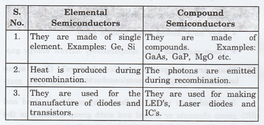
What are elemental semiconductors? Give some important elemental
semiconductors. (A.U Dec 2014)
Elemental
semiconductors are made from single element of the fourth group elements of the
periodic table.
Example : Germanium and silicon.
2.
What are the properties of semiconductors? (A.U. June 2013)
i.
They are formed by covalent bond.
ii.
They have empty conduction band.
iii.
They have almost filled valence band.
iv. These materials have comparatively narrow energy gap.
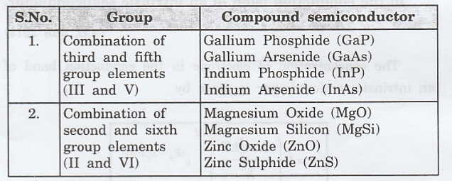
3.
What are compound semiconductors? Give some important compound semiconductors.
(A.U April 2015)
Semiconductors
which are formed by combining third and fifth group elements or second and
sixth group elements in the periodic table are called compound semiconductors.
4.
Mention any four advantages of semiconducting materials. (April 2013, April
2014)
i.
It behaves as insulator at 0 K and as conductor at high temperatures.
ii.
It has some properties of both conductor and insulator.
iii.
On doping, n and p-type semiconductors are produced with charge carriers of
electrons and holes respectively.
iv.
It has many applications in electronic field such as manufacturing of diodes,
transistors, LED's, IC etc.
5.
What are the differences between elemental semiconductors and compound
semiconductors? (A.U June 2012, April 2014, Dec 2015)
6.
Write an expression for the concentration of electrons in the conduction band
of an intrinsic semiconductor. (A.U. Jan 2014)
The
concentration of electrons in the conduction band of an intrinsic semiconductor
is given by
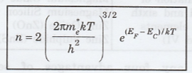
where
me* → effective mass of electron
EF
→ Fermi energy level
EC
→ Energy corresponds to the bottom of conduction band
T → Absolute temperature
7.
Write an expression for the concentration of holes in the valence band of an
intrinsic semiconductor. (A.U. May 2015)
The
concentration of holes in the valence band is given by
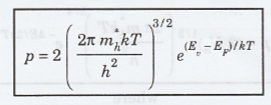
mh*
→ effective mass of hole
T
→ absolute temperature
EF
→ Fermi energy
Ev → Energy corresponds to the top of valence band
8.
Write an expression for carrier concentration in n-type semiconductor. (A.U. May 2015)
The
carrier concentration in n-type semiconductor is given by
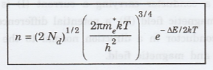
where
9.
Write an expression for carrier concentration of holes in the valence band of
p-type semiconductor. (A.U. Jan 2014)
The
carrier concentration in p-type is given by

10.
Define Hall-effect and Hall voltage. (A.U. May 2015, Dec 2016)
When
a conductor carrying a current (I) is placed in a transverse magnetic field
(B), a potential difference is produced inside the conductor in a direction
normal to the directions of the current and magnetic field.
This
phenomenon is known as Hall-effect and the generated voltage is called
Hall-voltage.
11.
Mention the uses of Hall effect. e uses of Hall effect (A.U. May 2013, June
2014)
i.
It is used to find type of semiconductor.
ii.
It is used to measure carrier concentration.
iii. It is used to find mobility of charge carrier.
iv.
It is used to measure the magnetic flux density using a semiconductor sample of
known Hall coefficient.
12.
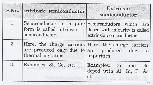
What are the differences between intrinsic and extrinsic semiconductor? (A.U
2008, June 2009, 2012)
13.
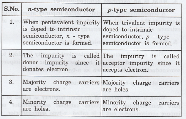
What are the differences between n-type and p-type semiconductor?
ADDITIONAL Q&A
1.
What is a semiconductor?
Semiconductor
is a special class of material which behaves like an insulator at 0 K and acts
as conductor at temperature other than 0 K. Its resistivity lies in between a
conductor and an insulator.
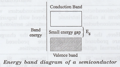
2.
Draw the energy level diagram of a semiconductor.
3.
What is an intrinsic semiconductor?
Semiconductor
in an extremely pure form (without impurities) is known as intrinsic
semiconductor.
4.
What is an extrinsic semiconductor?
A
semiconducting material in which impurity atoms added (doped) to the material
to modify its conductivity is known as extrinsic semiconductor or impurity
semiconductor.
5.
What is an n-type semiconductor?
When
a small amount of pentavalent impurity is added to a pure semiconductor, it
becomes extrinsic or impure semiconductor and it is known as n-type
semiconductor.
6.
What is a p-type semiconductor?
When a small amount of trivalent impurity is added to a pure semiconductor, it becomes extrinsic semiconductor or impure semiconductor and it is called p-type semiconductor.
7.
What is meant by doping and doping agent?
The
technique of adding impurities to a pure semiconductor is known as doping and
the added impurity is called doping agent.
8.
Explain the concept of hole in semiconductor.
In
intrinsic semiconductor, charge carriers are created due to breaking of
covalent bonds. When a covalent bond is broken, an electron escapes to the
conduction band leaving behind an empty space in the valence band. This missing
electron is called a hole.
9.
What is meant by donor energy level?
A
pentavalent impurity when doped with an intrinsic semiconductor donates one
electron which produces an energy level called donor energy level.
10.
What is meant by acceptor energy level?
A
trivalent impurity when doped with an intrinsic semiconductor accepts one
electron which produces an energy level called acceptor energy level.
11.
Mention the uses of compound semiconductor.
They
are used as photovoltaic materials, photoconductive cell, laser materials and
for making LED (Light Emitting Diode].
12.
Define drift velocity.
When
an electrical field is applied in a semiconducting material, the free charge
carriers such as free electrons and holes attain drift velocity vd
The
drift velocity attained by the carriers is proportional to the electrical field
strength E.
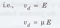
where
µ is a proportionality constant and it is known as the mobility of the charge
carrier.
13.
Define drift current.
The
electric current produced due to the motion of charge carriers under the
influence of an external electric field is known as drift current.
14.
Define diffusion current.
The
non-uniform distribution of charge carriers creates the regions of uneven
concentrations in the semiconductor.
The
charge carriers move from the regions of higher concentration to the regions of
lower concentration. This process is known as diffusion. The current is known
as diffusion current.
15.
What is a Hall device?
The
device which uses the hall effect for its application is known as Hall device.
16.
What are different types of Hall devices?
There
are three types of Hall devices.
They
are
(a)
Gauss Meter
(b)
Electronic Multiplier
(c)
Electronic Wattmeter
17.
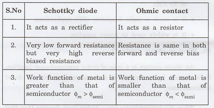
What is a schottky diode?
It
is a junction formed between a metal and n-type semiconductor.
When the metal has a higher work function than that of n-type semiconductor then the junction formed is called schottky diode.
18.
What are advantages of schottky diodes?
i.
In schottky diode, stored charges or depletion region is negligible. So a
schottky diode has a very low capacitance.
ii.
In schottky diode, the depleting region is negligible. So the schottky diode
will immediately switch from ON to OFF state (fast recovery time).
iii.
The depletion region is negligible in schottky diode. So applying a small
voltage is enough to produce large current.
iv.
It has high efficiency.
v.
It operates at high frequencies.
vi.
It produces less noise.
19.
What are the application of scholtky diode?
i.
Schottky diode can be used for rectification of signals of frequencies even
exceeding 300 MHz.
ii.
It is commonly used in switching device at frequencies of 20 GHz.
iii.
It is used in radio frequency (RF) applications.
iv.
It is widely used in power supplies.
20.
What is ohmic contact?
An
ohmic contact is a type of metal semiconductor junction. It is formed by a
contact of a metal with a heavily doped semiconductor.
When the semiconductor has a higher work function than that of metal, then the junction formed is called the Ohmic junction.
21.
What are the differences between schottky diode and p-n diode?

22.
What are the differences between schottky diode and ohmic contacts?
23.
What are the uses of ohmic contact?
The
use of ohmic contacts is to connect one semiconductor device to another, an IC,
or to connect an IC to its external terminals.
PART B (16 Marks Questions)
Anna University Questions:
Intrinsic semiconductor
1.
Obtain an expression for intrinsic carrier concentration in an intrinsic
semiconductor. (AU May 2014)
2.
Derive an expression for the density of holes in an intrinsic semiconductor.
(AU July, Dec. 2015)
3.
Derive an expression for concentration of holes (absence of electrons) in
intrinsic semiconductors. (AU Nov/Dec 2013)
4.
Obtain an expression for the carrier concentration of electrons in an intrinsic
semiconductor. (AU May/June 2014)
5.
Assuming the Fermi Dirac distribution derive an (8108 expression for the
concentration of electrons per unit volume in the conduction band of an
intrinsic semiconductor. (AU April/May 2014; Nov/Dec 2015)
Extrinsic semiconductors
6. Derive the relation for carrier
concentration in N type semiconductor. (AU Dec 2014)
7.
Obtain an expression for density of electrons in the conduction band of an n-
type and density of holes in the valence band of a p-type extrinsic
semiconductor. (AU Dec 2015)
8. Obtain an expression for the density of electrons in the conduction band of an n type semiconductors and show that it is proportional to the square root of the donor (concentration at low temperatures. Also state what happens at high temperatures. (AU Nov/Dec 2013)
9.
Obtain an expression for the density of holes in the valence type
semiconductors and show that it is proportional to the square root of the
acceptor concentration at low temperatures. (AU April/May 2012)
Hall
Effect
10.
(i) Give the theory of Hall effect.
(ii)
Using that effect how will you determine the electrical conductivity of a semiconductor.
(AU Oct 2014)
11.
(i) What is Hall effect? Derive an expression of Hall coefficient.
(ii)
Describe an experimental set-up for the measurement of the Hall voltage and
give its applications. (AU July 2015)
12. (i) What is Hall effect? Show that for a p
semiconductor the Hall coefficient RH is given by 1/pe
(ii)
Mention the applications of Hall effect. (AU Dec 2016)
13.
What is Hall effect? Give the theory of Hall effect. Describe the Hall effect
experiment to determine the Hall coefficient of semiconductor. (AU Dec 2013)
14.
(i) Obtain expression for Hall coefficient.
(ii)
How will you measure Hall coefficient experimentally?
(iii)
Describe any two applications of Hall effect. (AU May 2014)
15.
(i) Explain Hall effect in p-type and n-type semiconductors.
(ii)
Derive an expression for Hall coefficient.
(iii) Describe the experimental setup for the measurementof Hall coefficient. (AU, Dec 2016)
16. What is Hall effect? Derive an expression for Hall coefficient. Describe an experiment for the measurement of the Hall coefficient and mention its applications. (AU, May/June 2016)
17.
(i) Explain the phenomenon of Hall effect.
(ii)
Derive an expression for Hall coefficient for a n type semiconductor and for p
- type semiconductor. Also state how Hall voltage is related. (AU, May / June
2014)
Additional PART B (16 Marks
Questions)
1.
Derive an expression for electrical conductivity of intrinsic semiconductor.
2.
Write down the expression for drift current and diffusion currents.
3.
Explain working of any two Hall devices.
4.
Describe construction and working of scholtty diode.
5.
Write a note on ohmic contact.
ASSIGNMENT PROBLEMS
1.
In an intrinsic semiconductor, the effective mass of the electron is 0.07 mo
and that of the hole is 0.4 mo where mo is the rest mass
of the electron. Calculate the intrinsic concentration of charge at 300 K.
Given Eg = 0.7 eV [Ans: 2.3 x 10¹⁸/m3]
2.
In a Hall experiment, a current of 25 A is passed through a long foil of silver
which is 0.1 mm thick and 3 cm wide. A magnetic field of flux density 0.14 Wb/m2
is applied perpendicular to the foil. Calculate Hall voltage developed and
estimate the mobility of electrons in silver. Given the conductivity of silver
is 6.8 x 10⁷ Ω-1m-1 and Hall coefficient is - 8.4
x 10-11 m3/C. [Ans: 29.4 μV and μ = 57.7 × 10⁻⁴
m2 V-1 s-1]
Physics for Electronics Engineering: Unit III: Semiconductors and Transport Physics : Tag: : 2marks, 16marks, Assignment Problems | Physics for Electronics Engineering - Important Questions with Answers in Semiconductors and Transport Physics
Related Topics
Related Subjects

Physics for Electronics Engineering
PH3254 - Physics II - 2nd Semester - ECE Department - 2021 Regulation | 2nd Semester ECE Dept 2021 Regulation