Physics for Electronics Engineering: Unit III: Semiconductors and Transport Physics
Hall effect in n-type semiconductor
The electrical conductivity measurements are not sufficient for the determination of number of charge carriers and their mobilities.
HALL EFFECT
i. The electrical conductivity measurements are not sufficient for the determination of number of charge carriers and their mobilities.
ii.
Moreover, these measurements do not indicate whether current conduction is due
to electrons or holes.
iii.
Hence, it is very difficult to distinguish between p-type and n-type
semiconductors. Besides, the electrical conductivity measurements do not give
any information about the sign of the majority (p type or n type) charge
carriers.
iv.
Therefore, Hall effect is used to distinguish between two types of charge
carriers (electrons and hole). It also provides information about the sign of
charge carriers.
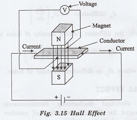
Statement
When
a conductor carrying a current (I) is placed perpendicular to a magnetic field
(B), (B), a potential difference is produced inside the conductor in a
direction perpendicular to both current and magnetic field. (Fig. 3.15)
This
phenomenon is known as Hall effect. The voltage thus generated is called Hall
voltage.
Hall effect in n – type semiconductor
Consider
a n-type semiconductor in the form of a rectangular slab. In this slab, the
current flows in X - direction and magnetic field B is applied in Z-direction.
Due to Hall effect, voltage is developed along Y - direction as shown in fig.
3.16.
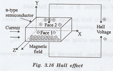
The
current flow is entirely due to the flow of electrons moving from right to left
along X-direction.
When
a magnetic field (B) is applied in Z-direction, then the electrons moving with
velocity v experience a downward force.
Downward
force experienced by the electrons = Bev
.................(1)
This
downward force deflects the electrons in downward direction. Hence, there is an
accumulation of negative charge (electrons) on the bottom face of the slab (fig
3.17).
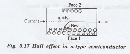
It
causes bottom face to be more negative with respect to top face.
Now,
a potential difference is developed between top and bottom faces of the slab.
This
potential difference produces an electric field EH in negative Y-
direction. It is called Hall field.
This
electric field develops a force (Lorentz force). This force is acting in the
upward direction on each electron.
Upward
force acting on each electron = eEH .................(2)
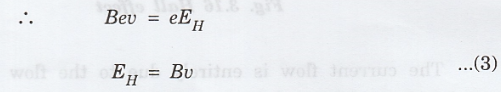
At
equilibrium, downward force balances upward force.
The
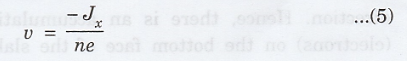
current density (Jx) along X-direction is related to velocity v as-
Jx = - nev
.................(4)
where
n is concentration electrons.
Substituting
eqn (5) in eqn (3), we have
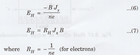
RH
is a constant and it is known as Hall coefficient.
The
negative sign indicates that the electric field is developed in negative Y-
direction.
Physics for Electronics Engineering: Unit III: Semiconductors and Transport Physics : Tag: : - Hall effect in n-type semiconductor
Related Topics
Related Subjects

Physics for Electronics Engineering
PH3254 - Physics II - 2nd Semester - ECE Department - 2021 Regulation | 2nd Semester ECE Dept 2021 Regulation