Physics for Electronics Engineering: Unit II: Electrical and Magnetic Properties of Materials
Quantum Interference Devices
SQUID, Transistor(QUIT), Magneto resistance(GMT)
When the magnetic field is applied perpendicular to the plane of the ring, the current is induced at the two Josephson junctions. The induced current produces the interference pattern and it flows around the ring so that the magnetic flux in the ring can have the quantum value of magnetic field applied.
QUANTUM INTERFERENCE DEVICES
SQUID
SQUID
stands for Superconducting QUantum Interference Device. It is an
ultra-sensitive instrument used to measure very weak magnetic field of the
order of 10-14 tesla.
Principle
We know that a small change in magnetic field produces variation in the quantum flux.
Description and Working
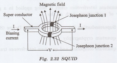
A
SQUID consists of a superconducting ring which can have magnetic fields of
quantum values (1, 2, 3...) of flux placed inbetween two Josephson junctions as
shown in fig. 2.32.
When
the magnetic field is applied perpendicular to the plane of the ring, the
current is induced at the two Josephson junctions. The induced current produces
the interference pattern and it flows around the ring so that the magnetic flux
in the ring can have the quantum value of magnetic field applied.
Application
i.
SQUID can be used to detect the variation of very minute magnetic signals in
terms of quantum flux.
ii.
It can also be used as storage device for magnetic flux.
iii.
SQUID is useful in the study of earthquakes, removing paramagnetic impurities,
detection of magnetic signals from the brain, heart etc.
Quantum Interference Transistor (QUIT):
Electrons are made to propagate through two arms of the quantum wire ring as shown in the fig. 2.33.
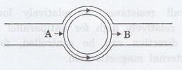
Fig. 2.33 A simple quantum wire
ring in which the interference of the electron waves at B controls the to
conductance of the device
Suppose
an electron wave enters the ring from left to right. The wave entering through
"A" gets split up into two partial waves. A constructive interference
can be expected to occur at "B" similar to the optical anlogue as
they travel through the same distance.
The
constructive interference at the output of the device reduces the resistance of
the ring. Various methods of introducing a phase difference of л between the
two waves have been suggested. This leads to destructive interference which in
turn will increase the resistance by reducing the current.
An
external voltage can control the nature of interference and the current. This
device is expected to act as a high-speed transistor.
Magneto resistance
Some
metallic materials show a large change in resistance on the application of a
magnetic field. This effect is called magneto resistance (MR).
Giant Magneto Resistance (GMR)
It
is a quantum mechanical magnetoresistance effect observed in multilayers
composed of alternating ferromagnetic and non-magnetic conductive layers.
Definition
The effect is observed as a significant change in the electrical resistance depending dion whether the magnetization of adjacent ferromagnetic layers are in a parallel or an antiparallel alignment.
The
overall resistance is alignment and relatively high for antiparallel alignment.
The magnetization direction can be controlled, for example, by applying an
external magnetic field.
The
effect is based on the dependence of electron scattering on the spin
orientation.
The
main application of GMR is magnetic field sensors, which used to read data in
hard disk drives, biosensors, microelectromechanical systems (MEMS) and other
devices. GMR multilayer structure are also used in magnetoresistive
random-access memory (MRAM) as cells that store one bit of information.
Explanation
The
GMR is seen in structures which have normal metal and ferromagnetic layers
alternatively. The electrical conductivity depends on the relative orientation
of magnetization in the successive ferromagnetic layers in the stack.
When
the relative magnetizations of the layers are switched from parallel (to the
plane of the layers) to antiparallel states, high and low resistivities are
obtained in the structure. This corresponds to 0 and 1 states in data storage
format.
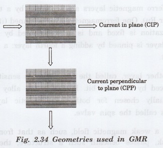
Two
geometries are commonly used in GMR studies and are as shown in fig. 2.34.
a.
Current in Plane (CIP) of layers and
b.
Current Perpendicular to Plane (CPP) of layers.
Since
the layers are only a few nanometers thick, the CIP mode offers high resistance
to the small cross sectional area encountered by the electrons.
To alter the resistivity by controlling the spin-dependent scattering, the lateral dimensions of the structure must be small when compared with the electron mean free path.
Physics for Electronics Engineering: Unit II: Electrical and Magnetic Properties of Materials : Tag: : SQUID, Transistor(QUIT), Magneto resistance(GMT) - Quantum Interference Devices
Related Topics
Related Subjects

Physics for Electronics Engineering
PH3254 - Physics II - 2nd Semester - ECE Department - 2021 Regulation | 2nd Semester ECE Dept 2021 Regulation