Physics for Electronics Engineering: Unit I: Crystallography
Pattern Alignment
Definition, Example | Crystallography
Pattern alignment is a process in which the mask patterns is aligned along different crystallographic directions. It also refers to alignment of mask pattern with respect to the pattern that already exists on the wafer.
PATTERN
ALIGNMENT
Pattern
alignment is a process in which the mask patterns is aligned along different
crystallographic directions. It also refers to alignment of mask pattern with
respect to the pattern that already exists on the wafer.
If the mask pattern is perfectly aligned
with respect to the pre-etched pattern it is termed as perfect alignment. If it
is not perfectly aligned then it is known as misalignment.
In the fabrication of MEMS (Micro
Electro Mechanical System) components, Bulk and Surface micromachining
processes basically involves several processing steps. Photolithography is one
of the major steps. These involve transferring of required pattern on the
substrate from the photo mask.
The exact structure of the desired
pattern mainly depends on two things.
(i) How accurately the mask edge is
aligned with the wafer flat.
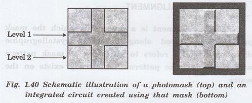
(ii) How accurately the wafer flat is
defined by the manufacturers. (Fig. 1.40).
Generally, (100), (110) and (111)
silicon wafers with different flat orientations such as <100>,
<110> and <111> are <110 and 11 a available in the market. These
are used to fabricate different types of MEMS structures on wafer surfaces. A
small degree of misalignment of the mask edge with the wafer flat results in
significant change in the final structure.
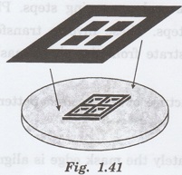
Example
Consider a photolithography process that
requires two layers of fabrication. The alignment marks used are a cross-type feature
in the first layer, and a square pattern in the second layer. When properly
aligned, the cross-type feature should fit inside the square pattern. (Fig.
1.41)
Physics for Electronics Engineering: Unit I: Crystallography : Tag: : Definition, Example | Crystallography - Pattern Alignment
Physics for Electronics Engineering: Unit I: Crystallography
Under Subject

Physics for Electronics Engineering
PH3254 - Physics II - 2nd Semester - ECE Department - 2021 Regulation | 2nd Semester ECE Dept 2021 Regulation
Related Subjects

Professional English II
HS3251 2nd Semester 2021 Regulation | 2nd Semester Common to all Dept 2021 Regulation
Statistics and Numerical Methods
MA3251 2nd Semester 2021 Regulation M2 Engineering Mathematics 2 | 2nd Semester Common to all Dept 2021 Regulation
Engineering Graphics
GE3251 eg 2nd semester | 2021 Regulation | 2nd Semester Common to all Dept 2021 Regulation
Physics for Electrical Engineering
PH3202 2nd Semester 2021 Regulation | 2nd Semester EEE Dept 2021 Regulation
Basic Civil and Mechanical Engineering
BE3255 2nd Semester 2021 Regulation | 2nd Semester EEE Dept 2021 Regulation
Electric Circuit Analysis
EE3251 2nd Semester 2021 Regulation | 2nd Semester EEE Dept 2021 Regulation
Physics for Electronics Engineering
PH3254 - Physics II - 2nd Semester - ECE Department - 2021 Regulation | 2nd Semester ECE Dept 2021 Regulation
Electrical and Instrumentation Engineering
BE3254 - 2nd Semester - ECE Dept - 2021 Regulation | 2nd Semester ECE Dept 2021 Regulation
Circuit Analysis
EC3251 - 2nd Semester - ECE Dept - 2021 Regulation | 2nd Semester ECE Dept 2021 Regulation
Materials Science
PH3251 2nd semester Mechanical Dept | 2021 Regulation | 2nd Semester Mechanical Dept 2021 Regulation

Basic Electrical and Electronics Engineering
BE3251 2nd semester Mechanical Dept | 2021 Regulation | 2nd Semester Mechanical Dept 2021 Regulation
Physics for Civil Engineering
PH3201 2021 Regulation | 2nd Semester Civil Dept 2021 Regulation
Basic Electrical, Electronics and Instrumentation Engineering
BE3252 2021 Regulation | 2nd Semester Civil Dept 2021 Regulation
Physics for Information Science
PH3256 2nd Semester CSE Dept | 2021 Regulation | 2nd Semester CSE Dept 2021 Regulation

Basic Electrical and Electronics Engineering
BE3251 2nd Semester CSE Dept 2021 | Regulation | 2nd Semester CSE Dept 2021 Regulation
Programming in C
CS3251 2nd Semester CSE Dept 2021 | Regulation | 2nd Semester CSE Dept 2021 Regulation