Physics for Electronics Engineering: Unit I: Crystallography
Example Use of Milliner Indices
Crystallography
Wafers are thin slices of semiconducting material widely used in the production of electronics and micro mechanical devices.
EXAMPLE
USE OF MILLINER INDICES
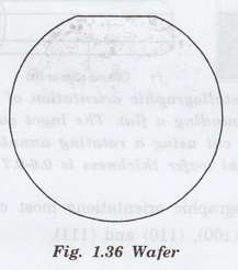
Wafer
Wafers
are thin slices of semiconducting material widely used in the production of
electronics and micro mechanical devices. In electronics, wafer
(also called slice substrate) is the crystalline silicon (C - Si) used to
manufacture integrated circuits and solar cells. (Fig.1.36)
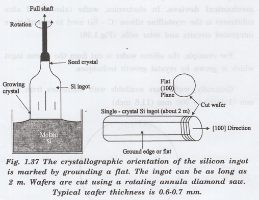
For example, the silicon wafer is cut
from the silicon ingot which is grown by crystal growth techniques.
Generally, wafers are available with
diameters from 25.4 mm (1 inch) to 300 mm (11.8 inch)
WAFER SURFACE ORIENTATION
The wafer surface is preoriented along a
specific crystallographic plane. A precise surface orientation is critical in
certain device processing steps. The orientation of crystalline materials
determines their optical, electrical and mechanical properties. (Fig. 1.37)
The growth plane of the crystalline
silicon orientations are described using Miller indices such as (100), (110),
(111), (211), etc. The different growth planes and orientations have different
arrangement of the atoms or lattice.
The crystallographic orientations most
commonly used in silicon wafer are (100), (110) and (111).
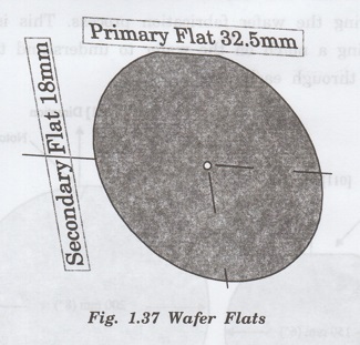
Wafer
flat and Notches
In order to identity a reference
direction within the surface plane of a wafer (i) Flat (ii) Notch is grounded
at the periphery at the pr of wafer.
WAFER FLATS
A wafer has a flat cut on one or more
sides at the periphery to indicate crystal direction as shown in fig. The large
and small values of flat cut are are typically set by wafer manufacturers. In
certain wafer double flat cuts are also made at the periphery.
Primary
Flat:
The flat of long length appearing in the
circumference of the wafer. The primary flat has a specific crystallographic
orientation relative to the wafer surface. (Fig. 1.37)
Secondary
Flat:
The flat of short length appearing in
the circumference of the wafer. This flat cut denotes type of wafer (either p
type or n type).
WAFER NOTCH
Instead of flat, a notch can also be
used to indicate crystallographic orientation of the wafer surface as shown in
fig. A notch a V-shaped of wafer. Usually, in silicon wafers the notch
indicates (011) direction of silicon.
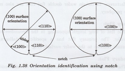
Importance
The position and orientation of a
semiconductor wafer is critical during the wafer fabrication process. This is
achieved by monitoring a notch on the wafer to understand the wafer's
orientation through each step.
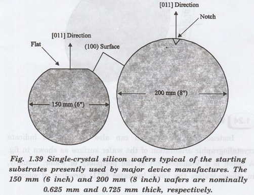
The facing surface is polished and
etched yielding a damage-free, mirror-like finish. The figure explains the use
of Miller indices in the (100) plane and (011) direction designations.
Physics for Electronics Engineering: Unit I: Crystallography : Tag: : Crystallography - Example Use of Milliner Indices
Physics for Electronics Engineering: Unit I: Crystallography
Under Subject

Physics for Electronics Engineering
PH3254 - Physics II - 2nd Semester - ECE Department - 2021 Regulation | 2nd Semester ECE Dept 2021 Regulation
Related Subjects

Professional English II
HS3251 2nd Semester 2021 Regulation | 2nd Semester Common to all Dept 2021 Regulation
Statistics and Numerical Methods
MA3251 2nd Semester 2021 Regulation M2 Engineering Mathematics 2 | 2nd Semester Common to all Dept 2021 Regulation
Engineering Graphics
GE3251 eg 2nd semester | 2021 Regulation | 2nd Semester Common to all Dept 2021 Regulation

Physics for Electrical Engineering
PH3202 2nd Semester 2021 Regulation | 2nd Semester EEE Dept 2021 Regulation
Basic Civil and Mechanical Engineering
BE3255 2nd Semester 2021 Regulation | 2nd Semester EEE Dept 2021 Regulation
Electric Circuit Analysis
EE3251 2nd Semester 2021 Regulation | 2nd Semester EEE Dept 2021 Regulation
Physics for Electronics Engineering
PH3254 - Physics II - 2nd Semester - ECE Department - 2021 Regulation | 2nd Semester ECE Dept 2021 Regulation
Electrical and Instrumentation Engineering
BE3254 - 2nd Semester - ECE Dept - 2021 Regulation | 2nd Semester ECE Dept 2021 Regulation
Circuit Analysis
EC3251 - 2nd Semester - ECE Dept - 2021 Regulation | 2nd Semester ECE Dept 2021 Regulation
Materials Science
PH3251 2nd semester Mechanical Dept | 2021 Regulation | 2nd Semester Mechanical Dept 2021 Regulation

Basic Electrical and Electronics Engineering
BE3251 2nd semester Mechanical Dept | 2021 Regulation | 2nd Semester Mechanical Dept 2021 Regulation
Physics for Civil Engineering
PH3201 2021 Regulation | 2nd Semester Civil Dept 2021 Regulation
Basic Electrical, Electronics and Instrumentation Engineering
BE3252 2021 Regulation | 2nd Semester Civil Dept 2021 Regulation
Physics for Information Science
PH3256 2nd Semester CSE Dept | 2021 Regulation | 2nd Semester CSE Dept 2021 Regulation

Basic Electrical and Electronics Engineering
BE3251 2nd Semester CSE Dept 2021 | Regulation | 2nd Semester CSE Dept 2021 Regulation
Programming in C
CS3251 2nd Semester CSE Dept 2021 | Regulation | 2nd Semester CSE Dept 2021 Regulation