Physics for Electronics Engineering: Unit I: Crystallography
Imperfections or Defects in Crystals
Definition, Classification
In an ideal crystal (perfect crystal), the atomic arrangement is perfectly regular and continuous throughout. But in real crystals due to some reasons the regular orientation of atoms may be disturbed at a point, along a line or in a region.
IMPERFECTIONS
IN CRYSTALS
In an ideal crystal (perfect crystal),
the atomic arrangement is perfectly regular and continuous throughout.
But in real crystals due to some reasons
the regular orientation of atoms may be disturbed at a point, along a line or
in a region.
Definition
The disturbance occurred in the regular
orientation of atoms is called crystal defect or imperfection.
The imperfections or defects are always
present in the actual crystal and their effects are often very important in
understanding the properties of crystals.
Some properties of crystal defects are
structure sensitive i.e., properties such as mechanical strength, ductility,
crystal growth, magnetic hysteresis, dielectric strength are greatly affected
by the relatively minor changes in crystal structure caused by the
imperfections.
Some other of properties crystals structure-insensitive i.e., properties
such as stiffness and density are not affected by the presence of
imperfections.
Classification of crystal imperfections (or Defects)
Crystalline imperfections are classified
on the basis of their geometry as follows:
1.
Point Defects
(a) Vacancies
(b) Interstitials
(c) Impurities
2.
Line Defects
(a) Edge dislocation
(b) Screw dislocation
3.
Surface Defects
(a) Grain boundaries
(b) Tilt boundaries
(c) Twin boundaries
(d) Stacking faults
4.
Volume Defects
Cracks
Point Defects
Point defects are crystalline
irregularities of atomic dimensions. They are imperfect points like regions in
the crystal. One or two atomic diametre is the typical size of a point
imperfection.
i. Point defects take place due to imperfect
packing of bas atoms during crystallisation.
ii. They produce distortion inside the
crystal structures.
iii. They produce strain only in its
surroundings but they tions do not affect the regularity in other parts of the
crystal.
Types
of point defects
The different types of point defects are
(a) Vacancies
(b) Interstitial
(c) Impurities
(a)
Vacancies
A vacancy is the simplest point defect
in a crystal. It refers to a missing atom or vacant atomic site.
Whenever one or more atoms are missing
from a normally occupied position as shown in fig 1.42, the defect caused is
known as vacancy.
Vacancies may be single as shown in
figure 1.42 or two or more of them.
These defects may arise due to imperfect
packing during original crystallisation and thermal vibrations of the atoms at
high temperatures.
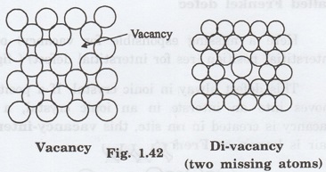
The atoms surrounding the vacancies are
displaced inwards thereby distorting the regularity of arrangement. There are
different kinds of vacancies like Frenkel
defect, Schottky defect, Colour center, etc.
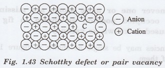
Schottky
defect
It refers to the missing of a pair of
positive and negative ions in an ionic crystal.
Here, two oppositely charged ions are
missing from an ionic crystal, therefore a cation-anion divacancy is created,
(fig. 1.43) This is known as schottky
defect or schottky imperfection
or iron pair vacancies. Since a pair
is missing, electrical neutrality is maintained.
Frenkel
Defect
A
vacancy associated with interstitial impurity is called Frenkel defect.
Here a missing atom (responsible for
vacancy) occupies interstitial position (responsible for interstitial defect)
(fig 1.44.)
This defect always occurs in ionic
crystal. If a positive ion moves into an interstitial site in an ionic crystal,
a cation vacancy is created in normal ion site, this vacancy-interstitial pair is known as Frenkel defect.
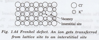
i. Frenkel defect does not change the
overall electrical neutrality of the crystal.
ii. The presence of these defects in
ionic crystals causes an increase in electrical conductivity.
(b)
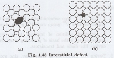
Interstitial defect
When
an extra atom occupies interstitial space (i.e., voids) within the crystal
structure without removing parent atom, the defect is called interstitial
defect.
An atom can enter into interstitial
space or void only if it is smaller than the parent atom otherwise it will
produce atomic distortion or strain because interstitial atom tends to push the
surrounding atoms further apart.
Types of interstitial defect
Interstitial defect has two types
(i) Self interstitial
(ii) Foreign interstitial
(i)
Self interstitial
If an atom from same crystal occupies
interstitial site, then it is called self interstitial. (Fig. 1.45 (a))
(ii)
Foreign interstitial
If an impurity atom (foreign atom)
occupies interstitial site, then it is called foreign interstitial. (Fig.
1.45(b))
(c)
Impurities
When
the foreign atoms (impurities) are added to crystal lattices, they are known as
impurities. The defect is called impurity defect.
The impurity atom may fit in the
structure in two ways giving rise to two kinds of impurity defects. They are
i. Substitutional impurity defect
ii. Interstitial impurity defect
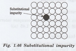
i. Substitutional impurity defect
A substitutional impurity refers to a
foreign atom that replaces a parent atom in the lattice (figure 1.46.)
Substitutional impurities change the
electrical properties enormously.
Example
1. n-type and p-type semiconductors have
substitutional impurities from th group and IIIrd group elements.
A controlled addition of impurity to a
very pure semiconductor is the basis of producing many electronic devices like
diode and transistors.
2. During the production of brass alloy,
zinc atoms are doped in copper lattice. Here, zinc atoms are called as
substitutional impurities.
ii. Interstitial impurity
An interstitial impurity is a small
small size size atom occupying the empty space (interstitial) in the parent
crystal, without dislodging any of the parent atoms from their sites (Fig.
1.47)
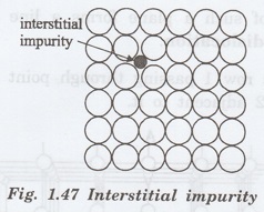
An atom can enter into interstitial or
empty space only when it is substantially smaller than parent atom.
Example.
In FCC iron, the atomic radius of iron atom is 0.225 nm. The carbon atoms with
atomic radius 0.078 nm can occupy empty spaces in FCC lattice as interstitial
impurities.
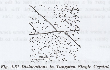
Line
Defects or Dislocations (One Dimensional Effect)
The defects due to dislocation or
distortion of atoms along a line are known as line defects.
These defects are also called
dislocations. In the geometrical sense, they are one dimensional defects.
In line defect, a portion of a line of
atoms is missing or displaced from its regular site.
Types of line defects
There are two types of line defects.
(a) Edge dislocation and
(b) Screw dislocation
(a)
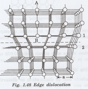
Edge dislocation
An edge dislocation arises when one of
the atomic planes forms only partially and does not extend through the entire
crystal (fig. 1.48.)
The atomic plane AB abruptly terminates
at B. It is viewed as an extra plane inserted in between a set of parallel
planes.
The edge of such a plane forms a line
defect and it is called an edge dislocation.
The atomic row 1 passing through point B
has one atom more than row 2 adjacent to it.
Classification
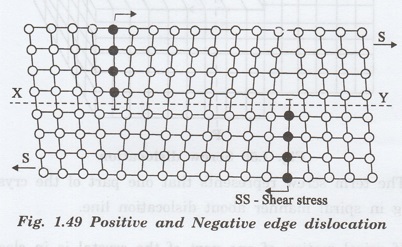
of edge dislocation
Edge dislocations are symbolically
represented by 1 or T depending on whether the incomplete plane starts from top
or bottom of the crystal.
These two configurations are referred as
i. Positive edge dislocation
ii. Negative edge dislocation
i. Positive edge dislocation
If the extra plane of atoms is above the
slip plane of the crystal than the edge dislocation is called positive as shown
in fig 1.49. It is denoted by the symbol 1.
ii. Negative edge dislocation
If the extra plane of atoms is below the
slip plane than the edge dislocation is called negative. (Fig. 1.49) It is
denoted by the symbol T.
(b) Screw
dislocation
Screw dislocation is due to displacement
of atoms in one part of a crystal relative to rest of the crystal. The
displacement terminates within crystal. This dislocation forms a spiral ramp
around dislocation line (Fig. 1.50).
In a screw dislocation, there is a line
of atoms about which crystal planes are warped to give an effect similar to
threads of a screw.
The row of atoms marking the termination
of the displacement is the screw dislocation. EF indicates the dislocation
line.
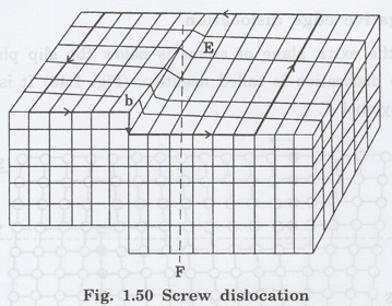
The term screw represents that one part
of the crystal is moving in spiral manner about dislocation line.
If spiral motion of one part of the
crystal is in clockwise direction then, dislocation is right handed, on the
other hand spiral motion is in anti-clockwise direction then, dislocation is
left handed.
Surface Defects (Plane Defects)
The defects on the surface of material
are called surface defects or plane defects.
They are also known as two dimensional imperfections.
Surface defects are due to a change in
the stacking of atomic planes on or across a boundary.
Some important internal surface defects
(i) Grain boundaries
(ii) Tilt and twist boundaries
(iii) Twin boundaries
(iv) Stacking fault
(i)
Grain boundaries
Whenever the grains of different
orientations separate the general pattern of atoms and exhibits a boundary, the
defect caused is called grain boundary. (Fig. 1.52)
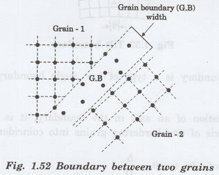
A grain boundary is formed when two
growing grain surfaces meet. The shape of the grain is usually influenced by
the presence of surrounding grains.
This type of defect generally takes
place during the solidification of liquid metal.
(ii)
Tilt and twist boundaries
Tilt boundary is another surface
imperfection. It is an array of parallel edge dislocations of same sign (i.e.,
either T or 1) arranged one above other in an array or series (figure 1.53)
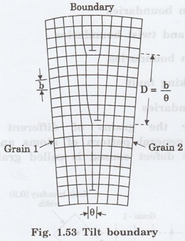
Tilt boundary is a type of low angle
boundary (i.e., less than 10°).
By rotation of an axis in the boundary,
it is possible to bring the axis of two bordering grains into coincidence, then
Angle of tilt, tan θ = b / D
D- Dislocation spacing
b = Length of Burger's vector
When is very small, then tan θ = θ
θ = b / D
Twist
boundaries
Twist boundaries are another type of low
angle boundaries. It consists of atleast two sets of parallel screw
dislocations lying in the boundary. In twist boundary, the rotation is about an
axis normal to the boundary.
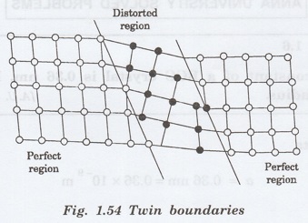
(iii)
Twin boundaries
Twin boundaries are another surface
imperfections.
If the boundaries in which the atomic
arrangement on one side of the boundary is somewhat a mirror image of the
arrangement of atoms of the other side (fig. 1.54). The defect caused is called
twin boundary.
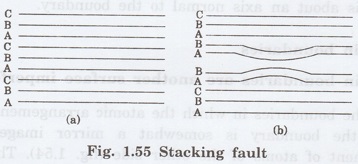
(iv) Stacking
Faults
It is a kind of surface imperfection.
Whenever the stacking of atoms is not in proper sequence throughout the
crystal, defect caused is called stacking fault.
Explanation
Fig. 1.55(a) shows the proper sequence
of atomic planes if we read from bottom to top as A - B - C - A - B - C - A - B
- C
But fig. 1.55 (b) shows the sequence of
atomic planes as A - B - C - A - B - A - B - A - B - C.
The region in which the stacking fault
occurs (A - B - A - B) forms a thin region of a hexagonal close packing in a
FCC crystal.
Physics for Electronics Engineering: Unit I: Crystallography : Tag: : Definition, Classification - Imperfections or Defects in Crystals
Related Topics
Related Subjects

Physics for Electronics Engineering
PH3254 - Physics II - 2nd Semester - ECE Department - 2021 Regulation | 2nd Semester ECE Dept 2021 Regulation