Physics for Electronics Engineering: Unit IV: Optical Properties of Materials
Optoelectronic Devices: Light Detectors
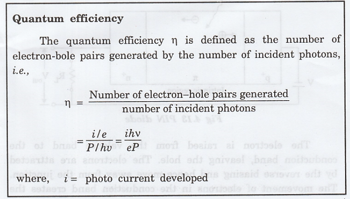
Definition, Types, Examples, Energy Band diagram, Efficiency
For processing the light signal at the receiver end of the fibre link we require a device to convert the light signals to electrical wave forms. This task is done by the photo-detectors.
OPTOELECTRONIC DEVICES
Optoelectronic devices play a vital role in the fiber optics communication, switching and logic gates. These are based on variation of optical parameters and subsequent electrical output. Optoelectronics combines the properties of light with the capabilities of electronics.
The
importance of optoelectronics applications results from the advances in
semiconductor materials, optical fiber communication, optical data processing,
display devices and data storage devices.
LIGHT DETECTORS
For
processing the light signal at the receiver end of the fibre link we require a
device to convert the light signals to electrical wave forms. This task is done
by the photo-detectors.
Definition
It
is a device which converts light signal into electrical wave forms.
Types of photo-detectors
Photo-detectors
are of three types:
(i)
Photo emissive
(ii)
Photo conductive
(iii)
Photo voltaic
(i) Photo-Emissive Photo-Detector
The
emission of electrons from a photo cathode by the incident photon is called
photo-emission.
Examples
of such devices
a.
Photo-tubes
b.
Photo-multiplier tubes
(The size of these is normally very large and hence not suitable for use as fibre optic detectors.
(ii) Photo-Conductive Devices
These
types of devices have variation of resistance due to incident light on the
photo-conductive materials.
Example
of photo-conductive materials
a.
Materials like CdS,
b.
Intrinsic semiconductor materials like PIS, PhTe
c.
Extrinsic semiconductor like doped Ge and Si
They
are not suitable for use in fibre optic communication purposes since they have
low frequency response.
(iii) Photo-Voltaic Devices
Semiconductor
junction photo diodes are called as photo-voltaic devices
They
are almost ideal for fibre systems. (0)
We
will study three forms of these devices.
1.
PN junction photo detector
2.
PIN photo diode
3.
Avalanche photo diode (APD)
PN
junction photo diode as in fig.4.12 explains the basic detection mechanism of a junction detector.
When reverse biased, the potential energy barrier between the p and n regions increases. Free electrons (which normally reside in the n region) and free holes (normally in the p region) cannot climb the barrier, so no current flows.
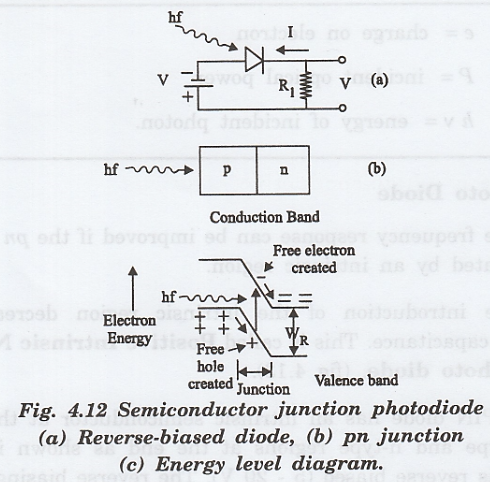
The
junction refers to the region where the barrier exists. Because there are no
free charges in the junction, it is called the depletion region.
Figure
4.12 shows an incident photon being absorbed in the junction after passing
through. the p layer. The absorbed energy raises a bound electron across the
bandgap.
PIN Photo Diode
The
frequency response can be improved if the pn junction is separated by an
intrinsic region.
The
introduction of the intrinsic region decreases the junction capacitance. This
is called Positive Intrinsic Negative (PIN) photo diode. (fig 4.13).
A
PIN diode has an intrinsic semiconductor at the centre and p-type and n-type
regions at the end as shown in figure 4.14. It is reverse biased (5 - 20 V).
The reverse biasing is used to attract the charge carriers from the intrinsic
regions.
When
light is incident on the PIN diode, the intrinsic region receives more amount
of light because of its large size. The photons incident on the the intrinsic
region produces electron-hole pair.
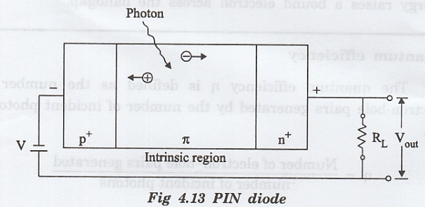
The electron is raised from the valence band to the conduction band, leaving the hole. The electrons are attracted by the reverse biasing and hence move away from the junction. The movement of electrons in the conduction band creates the
flow
of charge and hence the light energy gets converted into electrical energy.
Avalanche
Photo-Diodes (APD)
Fig
4.14 explains the working of Avalanche photo-diode. It is much more sensitive
than PN or PIN diodes.
The
avalanche photodiode is based on the principle of avalanche multiplication of
the current. It consists of heavily doped p+ and n+
regions.
The
depletion region is lightly doped, almost intrinsic. The diode is reverse
biased using 50-300 V. The light is made to incident on the depletion region.
The incident light produces electron and hole pair.
The
electrons move towards the p region. Due to the strong reverse biasing, there
is a depletion of charge carriers in the p region. The electrons in the p
region undergo avalanche multiplication because of high reverse bias.
The
holes move towards the p+ regions without producing further
multiplication.
The
avalanche photodiode has better noise performance, because the carrier
multiplication is limited to electrons only.
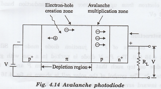
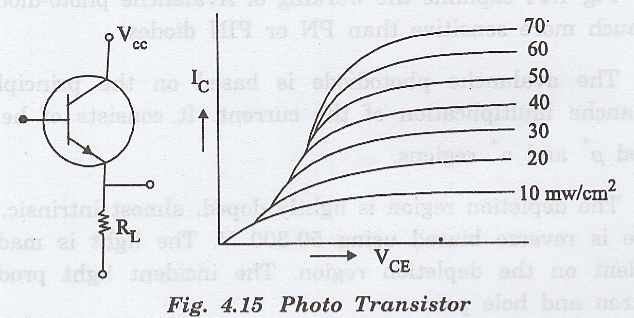
Photo-Transistor
Photo-Transistor
is another type of photo detector.
A
transistor photo diode with its characteristic curves is shown in fig. 4.15.
Physics for Electronics Engineering: Unit IV: Optical Properties of Materials : Tag: : Definition, Types, Examples, Energy Band diagram, Efficiency - Optoelectronic Devices: Light Detectors
Related Topics
Related Subjects

Physics for Electronics Engineering
PH3254 - Physics II - 2nd Semester - ECE Department - 2021 Regulation | 2nd Semester ECE Dept 2021 Regulation