Physics for Electronics Engineering: Unit IV: Optical Properties of Materials
Optical (Photonic) Switching
Types, Working Principle, Plasmon
The optoelectronic switching devices are very useful for computing and light activated logic gates applications. Optical photonic switching refers to a phenomenon in which transmission of an optical field through a device is switched among two or more possible states by optical means.
OPTICAL (PHOTONIC) SWITCHING
The
optoelectronic switching devices are very useful for computing and light
activated logic gates applications.
Optical photonic switching refers to a phenomenon in which transmission of an optical field through a device is switched among two or more possible states by optical means.
Types of optical switching
There
are two types of optical switching such as linear optical switching and non
linear optical switching. The Quantum Controlled Stark Effect (QCSE) in p - i
(Multi Quantum Well) -n (p – type - instrinsic - n - type) diode is used for
linear optical switching. optically controlled switching and logic devices are
based on the QCSE.
Quantum
confined stark effect refers to the bending of potential well due to transverse
applied electric field and shifting of the absorption edge of exciton to lower
energy side and resulting absorption of photons whose energy is less than the
original exciton absorption peak energy.
The
nonlinear optical switching is based on the self phase modulation (SPM).
The transmission of light through the device is intensity dependent so that the optical beam itself induces a switching depending on its intensity. This phenomenon is called self phase modulation and it exhibits in optical fiber.
In
a short piece of optical fiber, its ends are made highly reflecting through
suitable thin film coating. This device is used. to select a particular channel
in a multichannel optical communication system.
The
phase shift introduced by the above fiber depends on intensity and power of the
light beam. The nonlinear optical switching provides a faster switching time 10-15
second.
Self Electro Optic Effect Device (SEED)
In
p – i (MQW) – n diode, when the
reverse bias voltage increases to a large value, the tunneling current varies
remarkably as shown in fig.4.36.
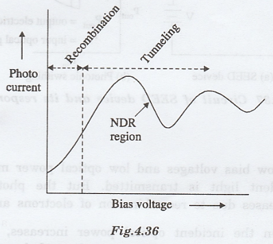
The photocurrent-bias voltage characteristic
curve, exihibits negative differential resistance (NDR) region (Fig.4.36). The
NDR occurs where the heavy-hole (HH) and the light-hole (LH) absorption peaks
cross the photon energy of the input light.
This NDR effect is exploited in SEED. Thus the SEED switching, bistability and optically induced oscillations.
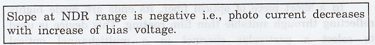
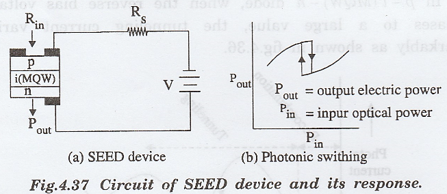
Fig.
4.37(a) shows the p – i (MQW) – n
diode in the reverse bias with a series resistor 'Rs'. Fig. 4.37(b),
shows input and output power response of the switching device, Pin
is incident optical power and Pout
= I2Rs is electric output power. Here I is the photo
current flowing r. Here is the photo current flowing through resistance Rs
Working:
i.
At low bias voltages and low optical power most of the incident light is
transmitted. But the photo current increases due to recombination of electrons
and holes.
ii.
When the incident optical power increases, the photo current(I) increases due
to tunneling of charge carriers. Thus the voltage drop I2Rs
across the series resistor increases.
iii.
Since the supply voltage remains constant, the negative bias across the diode
decreases. The heavy absorption peak is shifted to higher energies.
iv. Therefore the transmission of light is decreased. This will result more amount of light absorption and increased value of photo current due to tunneling.
v.
Thus the increase of the input optical power increases load the output electric
power as shown in fig.4.38
vi.
At particular input optical power, the heavy hole and iw light hole absorption
peaks cross the photon energy of the input light. Hence there is no absorption
of light by exciton or heavy hole or light hole.
Thus
the photo current decreases and correspondingly or an output electric power is
also decreased.
vii.
Thus the negative resistance region (NDR) arises as shown in fig. 4.36 and
4.37(b).
viii.
Further increase of input optical power increases the output electric power due
to ordinary photon absorption by the diode.
ix.
Thus the state of the device is altered by optical power. That is photonic or
optical switching is obtained by light beams with two different powers one for
complete transmission and other one for control (zero transmission of light).
x.
The hysteresis observed in the curve (Fig. 4.37(b)) is due to the asymmetric
shapes of the heavy hole and light 10 hole absorption curves. The feedback due
to the series resistor is optoelectronic type.
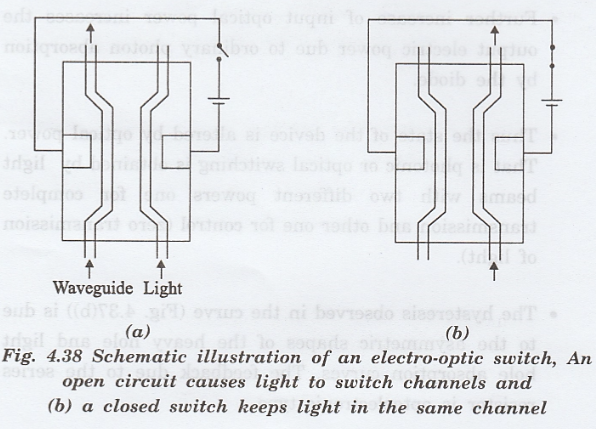
Electro-Optic Switch based on NLO
material
An example of an electro-optic switch based on NLO materials is shown in fig. 4.38. The switch is comprised of two parallel waveguides made of NLO materials.
The
waveguide channels have a different refractive index from the surrounding
material. The light can be switched back and forth between the channels by
applying and removing a voltage across the bottleneck. In the absence of an
electric field, the light travelling through the lower waveguide interacts with
the upper waveguide in a non-linear manner at the bottleneck, causing the light
to switch channels.
Switching does not occur when an electric
field is applied. The electric field polarizes the NLO material and alters the
refractive indices of the two channels, such that the non-linear interaction at
the bottleneck is modified and the light stays in the lower waveguide.
Plasmon
A plasmon is a quantum of plasma oscillation. Just as light (an optical oscillation) consists of photons, the plasma oscillation consists of plasmons.
The
plasmon can be considered as a quasiparticle since it arises from the
quantization of plasma oscillations.
Thus,
plasmons are collective oscillations of the free electron gas density. For
example, at optical frequencies, plasmons can couple with a photon to create
another quasiparticle called a plasmon polariton.
Physics for Electronics Engineering: Unit IV: Optical Properties of Materials : Tag: : Types, Working Principle, Plasmon - Optical (Photonic) Switching
Related Topics
Related Subjects

Physics for Electronics Engineering
PH3254 - Physics II - 2nd Semester - ECE Department - 2021 Regulation | 2nd Semester ECE Dept 2021 Regulation