Electronic Devices and Circuits: Unit II: Amplifiers
MOSFET Small Signal Model
Steps Involved in Small-Signal Analysis of MOSFET,
Small signal parameters are controlled by the Q-point. For the same operating point, MOSFET has lower transconductance and an output resistance that is similar to the BJT.
MOSFET SMALL SIGNAL MODEL
The
small signal model of MOSFET can be obtained similar to JFET. Fig.2.23 shows
the small signal equivalent circuit of MOSFET.

Since
gate is insulated from channel by gate-oxide, input resistance of transistor is
infinite.
i. Small signal parameters are controlled by the Q-point. For the same operating point, MOSFET has lower transconductance and an output resistance that is similar to the BJT.
ii.
In saturation mode, MOSFET acts as a voltage controlled current source. The
control voltage is VGS an the output current is iD.
STEPS INVOLVED IN SMALL-SIGNAL ANALYSIS OF MOSFET
Step 1:
Complete a DC analysis
The
goal of this DC analysis is to determine
(a)
the dc voltage VGS for MOSFET
(b)
the de voltage VDS for MOSFET
Step 2:
Calculate the small signal circuit parameters for the MOSFET.
Step 3:
Replace all MOSFETs with their small-signal circuit model.
Step 4:
Set all dc sources to zero.
Step 5:
Analyze small-signal circuit.
MOSFET COMMON SOURCE SMALL-SIGNAL AMPLIFIER ANALYSIS
The
common source MOSFET amplifier is shown in Fig.2.24.
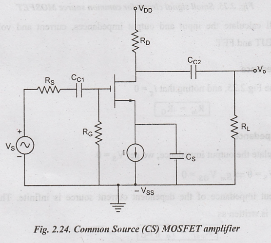
Construction
CC1
and CC2 are the coupling capacitors and the capacitor CS
is bypass capacitor. The capacitance values are chosen to be large so that
their reactances are very small at the operating frequency.
Analysis
Fig.
2.25 shows the small signal equivalent circuit for the common source MOSFET
amplifier.
We
will calculate the input and output impedances, current and voltage gain
similar to BJT and FET.
Input Impedance
From
the Fig.2.25, and noting that ig = 0

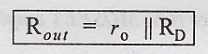
Output Impedance
To
calculate the output impedance, we get VS = 0
When
VS = 0 ⇒
gm VGS = 0
The
input impedance of the dependent current source is infinite. Thus output
impedance is written as
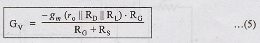
Voltage Gain
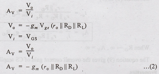
Overall Voltage Gain
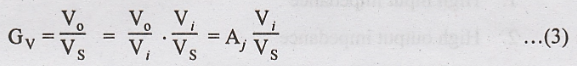
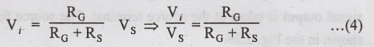
Applying
voltage division rule
Substitute
Rin = RG from input impedance (1)
Substitute
(4) in (3)
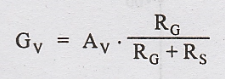
Substitute
(2)
Current Gain
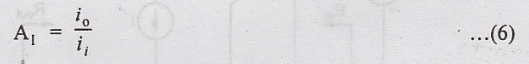
Using
current division rule
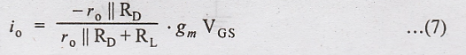
At
the input, 
Substitute
(8) in (7)
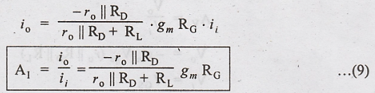
When
RG → ∞, AV = ∞
The
equation (9) gives the overall current gain of CS amplifier.
Properties
i.
High input impedance
ii.
High output impedance
iii.
Relatively high small-signal voltage gain
iv.
Very high small-signal current gain
Electronic Devices and Circuits: Unit II: Amplifiers : Tag: : Steps Involved in Small-Signal Analysis of MOSFET, - MOSFET Small Signal Model
Related Topics
Related Subjects

Electronic Devices and Circuits
EC3353 - EDC - 3rd Semester - ECE Dept - 2021 Regulation | 3rd Semester ECE Dept 2021 Regulation