Electronic Devices and Circuits: Unit II: Amplifiers
Common Base(CB) Amplifier Analysis
Construction, Operation, Characteristics, Application
The base terminal is common between the input and output circuit. The input is applied to emitter terminal and output is taken from the collector terminal.
COMMON BASE (CB) AMPLIFIER ANALYSIS
The
base terminal is common between the input and output circuit. The input is
applied to emitter terminal and output is taken from the collector terminal.
Construction
The
common base amplifier is shown in Fig. 2.19. The potential divider bias is
applied through resistors R1 and R2.
i.
The load resistor RL is connected to transistor collector terminal.
ii.
The signal source is coupled to the transistor emitter through C2.
iii.
Capacitor C1 constitutes an ac short circuit from the base terminal
to ground. So, all the input voltage appear across base emitter junction.
iv.
Capacitor C3 acts as coupling capacitor and it prevents the loading
effect due to RC and RL.
Operation
i.
During positive half of input signal, the emitter terminal is positive and the
base remains at a constant potential.
ii.
Therefore, a positive - going signal reduces base-emitter voltage VBE
which in turn reduces collector current IC. Thus the voltage drop
across the collector resistor also decreases.
Apply
KVL to the output circuit
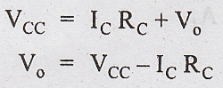
If
IC reduces, then VO ≈ VCC and there is no
phase shift between the input and output.
i.
During negative half cycle of input, the emitter terminal is negative. Thus
forward bias across Base-Emitter junction increases which in turn increases the collector current.
ii.
The voltage drop across RC increases ie IC RC
> VO. Thus the output voltage (VO = VCC IC
RC) decreases, and the output is negative value.
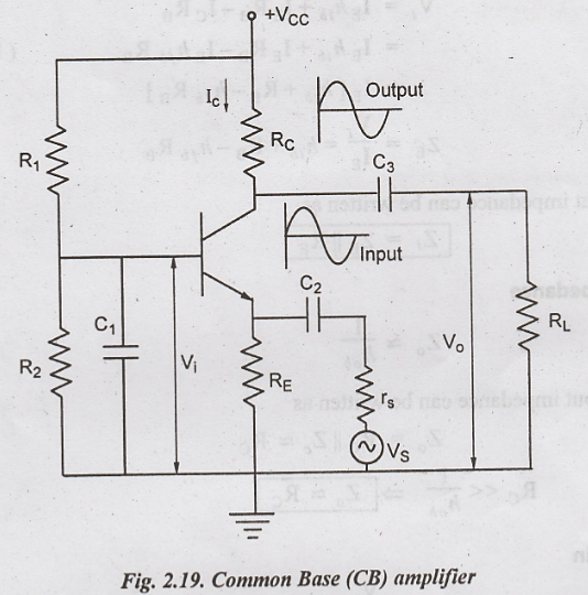
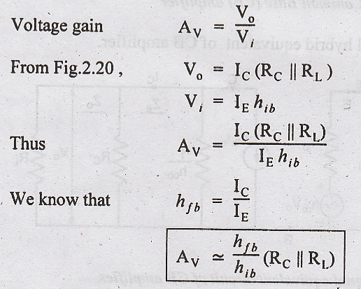
Fig.2.20
shows the small signal hybrid equivalent of CB amplifier.
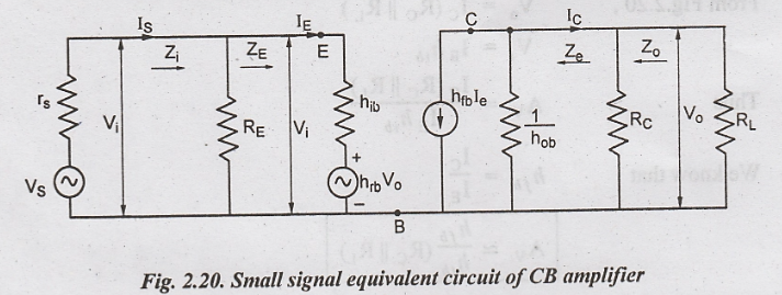
In this circuit, only a fraction of output voltage is fed back to input i.e. hrb is very small and can be neglected.
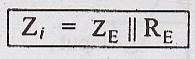
Input Impedance
Apply
KVL to Fig. 2.20,
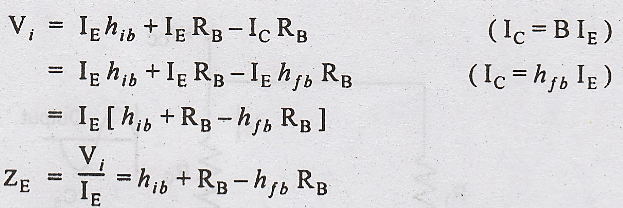
The
input impedance can be written as
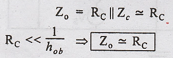
Output Impedance
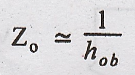
The
output impedance can be written as
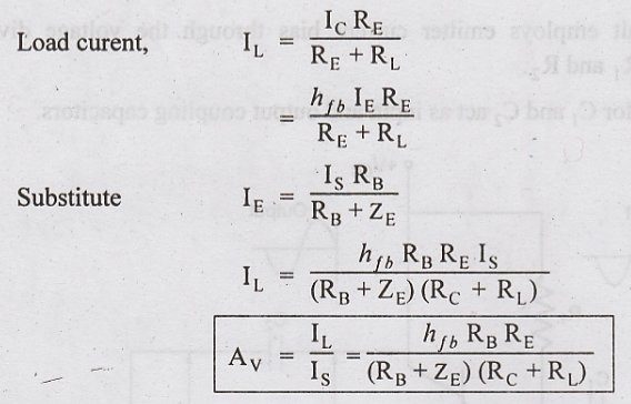
Voltage Gain
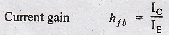
Current Gain
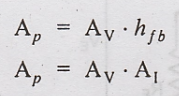
Power Gain
Characteristics of CB Amplifier
i.
provides voltage gain and power gain
ii.
High output impedance and very low input impedance
iii.
No current gain
Application
i.
High frequency voltage amplifier
Electronic Devices and Circuits: Unit II: Amplifiers : Tag: : Construction, Operation, Characteristics, Application - Common Base(CB) Amplifier Analysis
Electronic Devices and Circuits: Unit II: Amplifiers
Under Subject

Electronic Devices and Circuits
EC3353 - EDC - 3rd Semester - ECE Dept - 2021 Regulation | 3rd Semester ECE Dept 2021 Regulation
Related Subjects
Random Process and Linear Algebra
MA3355 - M3 - 3rd Semester - ECE Dept - 2021 Regulation | 3rd Semester ECE Dept 2021 Regulation

Signals and Systems
EC3354 - 3rd Semester - ECE Dept - 2021 Regulation | 3rd Semester ECE Dept 2021 Regulation
Electronic Devices and Circuits
EC3353 - EDC - 3rd Semester - ECE Dept - 2021 Regulation | 3rd Semester ECE Dept 2021 Regulation
Control Systems
EC3351 - 3rd Semester - ECE Dept - 2021 Regulation | 3rd Semester ECE Dept 2021 Regulation
Digital Systems Design
EC3352 - DSD - 3rd Semester - ECE Dept - 2021 Regulation | 3rd Semester ECE Dept 2021 Regulation