Electronic Devices and Circuits: Unit II: Amplifiers
Load Line and Operating Point
Biasing
The process of giving proper supply voltages and resistances for obtaining the desired operating point is known as biasing.
LOAD LINE AND OPERATING POINT
BIASING
The process of giving proper supply voltages and resistances for obtaining the desired operating point is known as biasing.
These voltages and resistances results in a set of dc voltage VCEQ and current ICQ to operate the transistor in the active region. These voltages and currents are called quiescent values and they determine the operating point or Q-point for the transistor.
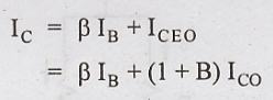
Since the operating point is a fixed point on the transistor characteristics, it is also called as Quiescent point or Q-point. The circuits used for getting the desired and proper operating point are known as biasing circuits. For faithful reproduction of input signal, the transistor should be operated in active region. The collector current for CE amplifier is given by
the variables β, IB and ICO increase with temperatures .For every 10°C increase in temperature, ICO doubles itself which leads to increase in IC.. This in turn increases power dissipation and increases ICO.
This in turn cause IC to increase further and becomes cumulative which leads to thermal runaway. It will destroy the transistor. Also, the Q-point can shift due to change in temperature and the transistor enter into saturation region.
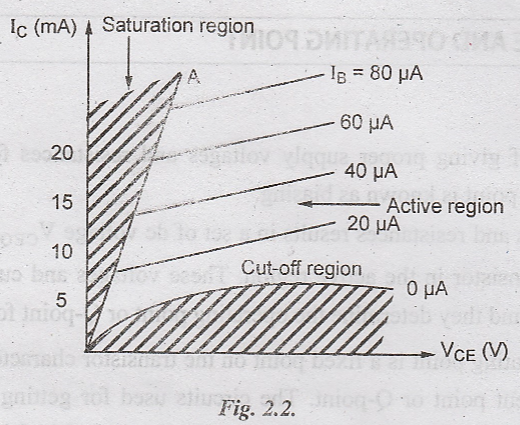
Consider the output characteristics of CE amplifier shown in Fig.2.2.
The transistor should meet the following conditions for good amplification.
1. Emitter base junction must be forward biased and collector base junction must be reverse biased.
2. VCE > VCE (sat) for any part of input signal.
3. IC = IC (max) if no signal is applied.
4. Maximum rating of the transistor IC(max), VCE(max) should not be exceeded at any value of input signal.
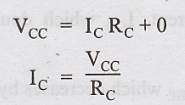
Consider the Fig.2.3, the values of VCE and RC are fixed.
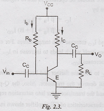
IC and VCE are dependent in RB.
Apply KVL to the collector circuit,

Substitute VCE = 0
Hence, the coordinates of A in Fig. are VCE = 0 and IC = VCC / RC
Substitute IC = 0 in equation (1)
VCE = VCC
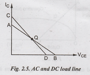
So, coordinates of B are VCE = VCC and IC = 0. Thus the dc load line AB can be drawn if RC and VCC values are known the straight line represented by AB in Fig. is known as dc load line.
When a value for maximum possible collector current is considered, the point in Y-axis is known as saturation point. When maximum possible collector emitter voltage is considered, the point in X axis is known as cut off point.
A line joining saturation point and cutoff point is known as Load Line. It indicates the output at the load.
The point at which these two lines intersect is known as operating point or Q- point.

A transistor acts as a good amplifier in active region. When it is operated at Q-point faithful amplification is achieved
The optimum point is located at the midpoint between A and B. The Q point should be fixed properly. If Q point gets shifted nearer to either A or B, then the output voltage and current will be clipped and output signal will be distorted.
Q-point shift occurs depending on
1. Reverse saturation current, ICO which doubles for every 10°C rise in temperature.
2. Base emitter voltage, VBE which decreases by 2.5mW per degree celcius.
3. Transmitter current gain, β which increases with temperature.
AC Load Line
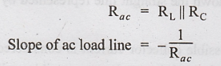
The operating point is selected by drawing dc load line. This point is chosen under zero input signal condition of the circuit. Therefore ac load line also pass through the operating point. The effective ac load resistance is given by

VCE (max) locates point D on VCE axis and ICEQ (max) locates point C on IC axis and ac load line CD is obtained by joining points C and D.
The dc load line is less steep than ac load line as RC > Rac
Stability Factor S
Stability factor helps to indicate the maintenance of operating point i.e it implies the degree of change in operating point due to change in temperature.

S should be small to have better thermal stability.
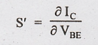
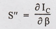
Stability factor S' and S".
S' is defined as the rate of change of IC with VBE, while IC and IBE are kept constant.
S" is defined as the rate of change of IC with β, with ICO and VBE kept constant.
Electronic Devices and Circuits: Unit II: Amplifiers : Tag: : Biasing - Load Line and Operating Point
Related Topics
Related Subjects

Electronic Devices and Circuits
EC3353 - EDC - 3rd Semester - ECE Dept - 2021 Regulation | 3rd Semester ECE Dept 2021 Regulation