Electronic Devices and Circuits: Unit II: Amplifiers
Gain and Frequency Response of High Frequency Analysis
Gain and Frequency Response of BJT Amplifier, Gain and Frequency Response of FET Amplifier
All the coupling and bypass capacitors have been assumed to be short circuited and wiring capacitance is ignored.
GAIN AND FREQUENCY RESPONSE OF HIGH FREQUENCY ANALYSIS
GAIN AND FREQUENCY RESPONSE OF BJT AMPLIFIER
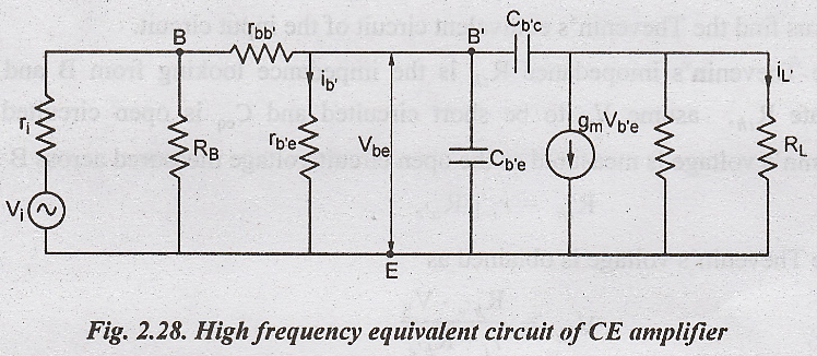
Fig.2.28
shows the high frequency equivalent circuit of CE amplifier. All the coupling
and bypass capacitors have been assumed to be short circuited and wiring
capacitance is ignored.
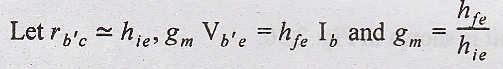
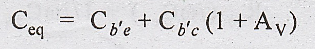
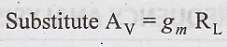
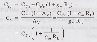
The
Fig. 2.29, can be simplified using Millers theorem as follows.
The
input and output feedback capacitance Cb'c are replaced by the input
and output shunting capacitances. Fig. 2.29 shows the modified circuit of CE
amplifier.
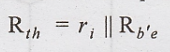
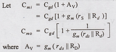
Let
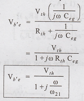
us find the Thevenin's equivalent circuit of the input circuit.
The
Thevenin's imopedance Rth is the impedance looking from B and E. To
calculate Rth asume VS to be short circuited and Ceq
is open circuited. Then Thevenin's voltage is measured as the open circuit
voltage measured across B and E.
The
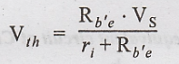
Thevenin's voltage is obtained as
The
simplified Thevenin's circuit is shown Fig.2.30.
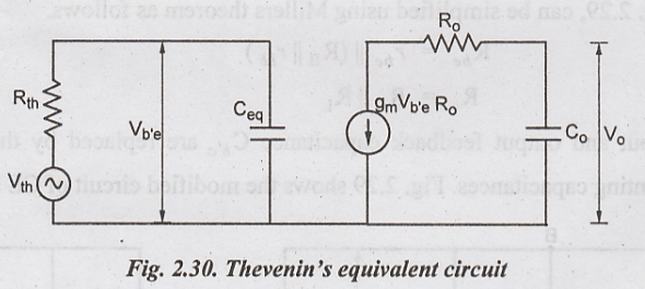
From
the Thevenin's equivalent circuit,
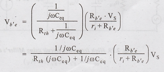
where 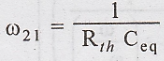 = upper 3dB cutoff frequency of input circuit
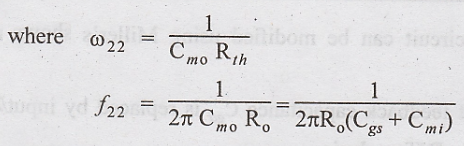
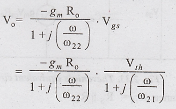
Consider
the output circuit,
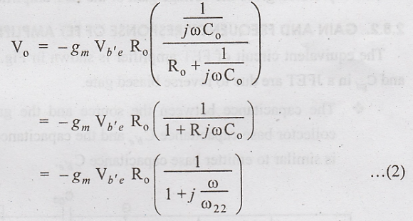
Where 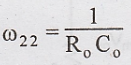 = upper 3 dB cutoff frequency of output circuit
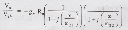
We
know that voltage gain, 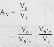
Substitute
(1) and (2)
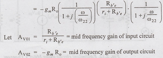
Hence
AV can be written as
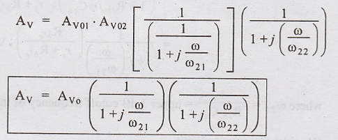
This
expression gives the voltage gain of the BJT amplifier.
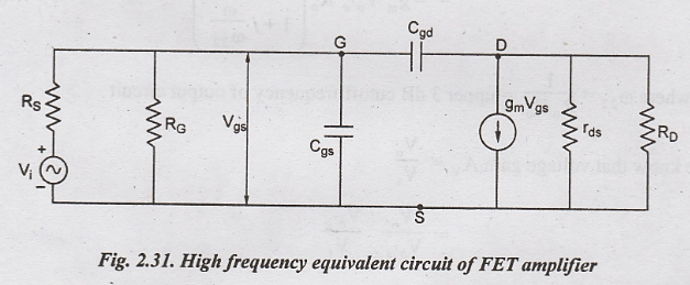
GAIN AND FREQUENCY RESPONSE OF FET AMPLIFIER
The
equivalent circuit of FET amplifier is shown in Fig.2.31. The capacitors Cgs
and Cgd in a JFET are due to reverse biased gate.
i.
The capacitance between the source and the gate Cgs is similar to the
collector base capacitance Cb'e and the capacitance between drain
and gate is similar to emitter base capacitance Cb'e
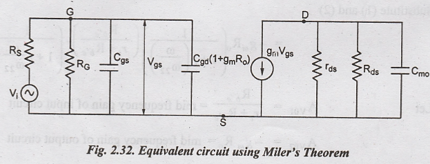
This
equivalent circuit can be modified using Miller's Theorem as shown in Fig.2.32.
The input/output feedback capacitance Cgd is replaced by input/output shunting capacitance similar to BJT analysis.
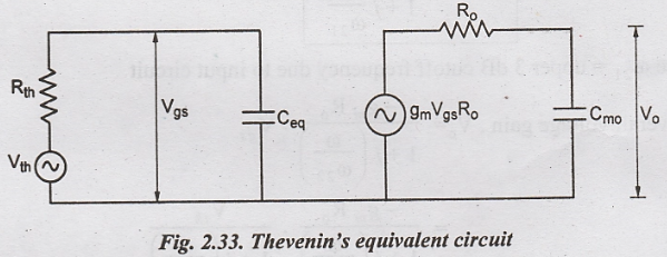
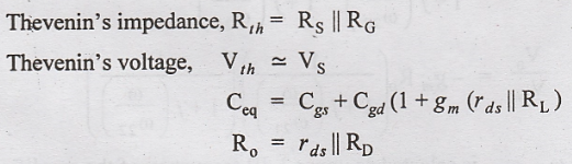
The
Thevenin's equivalnt circuit for the above circuit is obtained as shown in
Fig.2.33.
Applying
voltage division rule,
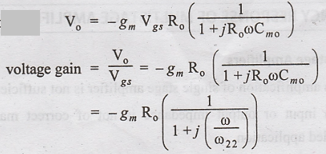
The
output voltage,
Applying
voltage division rule to the input circuit
Where
ω21 = upper 3 dB cutoff frequency due to input circuit
Overall
voltage gain,
The
lowest value of ω21, ω22 is selected as upper 3 dB frequency of the amplifier.
Electronic Devices and Circuits: Unit II: Amplifiers : Tag: : Gain and Frequency Response of BJT Amplifier, Gain and Frequency Response of FET Amplifier - Gain and Frequency Response of High Frequency Analysis
Related Topics
Related Subjects

Electronic Devices and Circuits
EC3353 - EDC - 3rd Semester - ECE Dept - 2021 Regulation | 3rd Semester ECE Dept 2021 Regulation