Electronic Devices and Circuits: Unit II: Amplifiers
Common Collector Amplifier
Comparison of CE CB and CC Amplifiers
The collector terminal is common between the input and output terminals. The input is applied at the base and the output is taken across the emitter terminal.
COMMON COLLECTOR
AMPLIFIER
The
collector terminal is common between the input and output terminals. The input
is applied at the base and the output is taken across the emitter terminal.
Construction
i.
The collector base junction acts as input and emitter base junction acts as
output.
ii.
The output voltage exactly follows the input voltage variations. Hence it is
called "Emitter follower" amplifier.
iii. The load resistor RL is capacitor coupled to the emitter terminal of the transistor.
iv.
The circuit employs emitter current bias through the voltage divider resistors
R1 and R2.
The
capacitor C1 and C2 act as input and output coupling
capacitors.
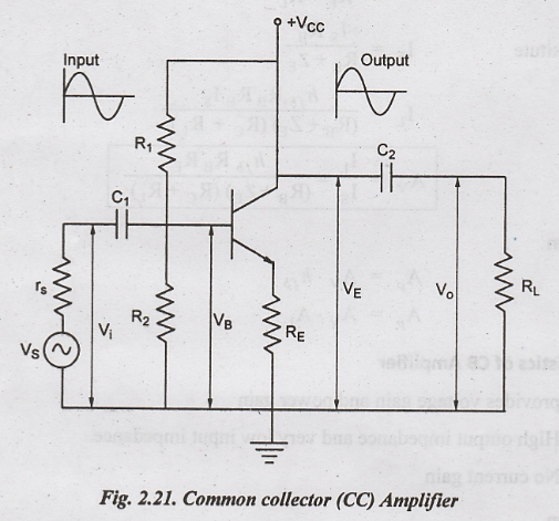
Operation
i.
When an ac signal is applied to transistor base via C1, VB
is increased and decreased as the signal varies from positive to negative
voltage variations.
VB
– VBE
ii.
Thus the output voltage from a common collector circuit is same as its input
voltage. So the CC amplifier has unity voltage gain.
Analysis of Emitter Follower Amplifier
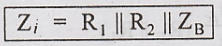
Input Impedance
From
Fig.2.22, Applying KVL
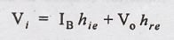
The
Input voltage
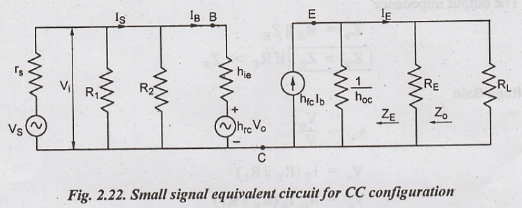
Substitute
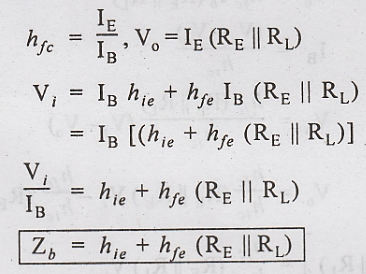
The
input impedance is given by
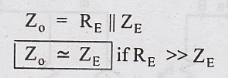
Output Impedance
The
input signal is assumed to be zero

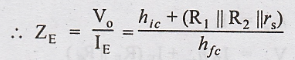
The
output impedance
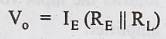
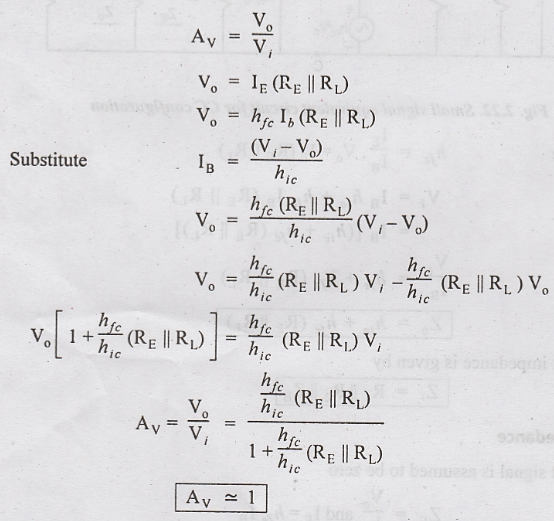
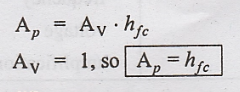
Voltage Gain
Current Gain
Current gain
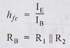
Applying
current division rule,
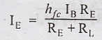
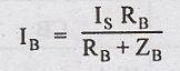
Substitute
IB value in IE
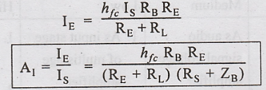
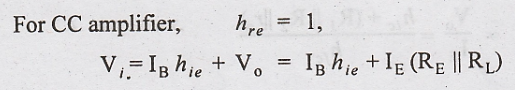
for
CC amplifier RB >> ZB
Power Gain
Characteristics of CC Amplifier
i.
Provides current gain and power gain
ii.
high input impedance and very low output impedance
iii.
No voltage gain.
Applications
1.
As buffer amplifier since voltage gain is unity
COMPARISON OF CE, CB AND CC AMPLIFIERS


Electronic Devices and Circuits: Unit II: Amplifiers : Tag: : Comparison of CE CB and CC Amplifiers - Common Collector Amplifier
Related Topics
Related Subjects

Electronic Devices and Circuits
EC3353 - EDC - 3rd Semester - ECE Dept - 2021 Regulation | 3rd Semester ECE Dept 2021 Regulation