Electronic Devices and Circuits: Unit II: Amplifiers
CE Amplifier with Emitter Resistor and Bypass Capacitance
h-parameter model, Characteristics of CE Amplifier, Applications
Characteristics of CE Amplifier: i. Good voltage gain ii. Phase inversion i.e., output voltage is 180° out of phase with input iii. Good current gain and power gain iv. High input and output impedance
CE AMPLIFIER WITH EMITTER
RESISTOR AND BYPASS CAPACITANCE
A
common emitter amplifier circuit is shown in Fig.2.17, the circuit consists of
biasing resistors R1 and R2, the temeprature
stabilization resistor RE collector resistor RC.
The
bypass capacitor 'C' is used to eliminate ac degeneration ie it bypass all ac
signal and increase the output gain.
i. The coupling capacitor C1 connects the signal source with the transistor base. C2 couples external load resistor RL to the collector of transistor.
ii.
C1 and C2 avoids the loading effect between input and
output.

Operation
When
the input voltage is increased in positive direction, VBE is
increased. Thus collector current IC increases, the voltage drop
occurs across RC.

Apply
KVL to collector circuit,


Input Impedance

Apply
KVL to input circuit

We know that

Output Impedence
Looking
into emitter and collector terminal

The
output impedance is given by

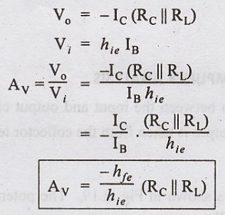
Voltage gain

Current Gain

Load Current

Power Gain

Characteristics of CE Amplifier
i.
Good voltage gain
ii.
Phase inversion i.e., output voltage is 180° out of phase with input
iii.
Good current gain and power gain
iv. High input and output impedance
Applications
i.
Voltage amplifier
Electronic Devices and Circuits: Unit II: Amplifiers : Tag: : h-parameter model, Characteristics of CE Amplifier, Applications - CE Amplifier with Emitter Resistor and Bypass Capacitance
Related Topics
Related Subjects

Electronic Devices and Circuits
EC3353 - EDC - 3rd Semester - ECE Dept - 2021 Regulation | 3rd Semester ECE Dept 2021 Regulation