Electronic Devices and Circuits: Unit II: Amplifiers
Biasing the FET
For the proper functioning of a linear FET amplifier, it is necessary to maintain the operating point Q stable in the central portion of the pinch off region. The Q point should be independent of device parameter variations and ambient temperature changes.
BIASING THE FET
For
the proper functioning of a linear FET amplifier, it is necessary to maintain
the operating point Q stable in the central portion of the pinch off region.
The Q point should be independent of device parameter variations and ambient
temperature changes. This can be achieved by suitably selecting the gate to
source voltage (VGS) and drain current (ID) which is
referred to as biasing.
An
FET may have combination of self bias and fixed bias to provide stability of
the quiescent drain current against device and temperature variations.
Self-Bias
Fig.
2.9 shows the self bias circuit for N-channel FET. When the drain voltage VDD
is applied, a drain current ID flows even in the absence of gate
voltage (VG). The voltage drop across resistor RS
produced by the drain current is given by VS = ID RS.
This voltage drop reduces the gate to source reverse voltage required for FET
operation. The resistor RS, the feedback resistor prevents any
variation in FET drain current.
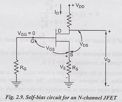
When
drain current increases, the voltage drop across RS increases. The
increased voltage drop increases the reverse gate to source voltage, which
decrease the effective width of the channel and hence, reduces the drain
current. Now the reduced drain current decreases the gate to source voltage
which, in turn increase the effective width of the channel thereby increasing
the value of drain current.
Voltage Divider Bias
Fig.
2.10 (a) shows the voltage divider bias circuit and it's Thevenin's equuivalent
is shown in Fig. 2.10(b). Resistors R1 and R2 connected
on the gate side forms a voltage divider. The gate voltage
The
bias line satisfies the equation VGS - VGG - ID
RS
The
drain to ground voltage, Vd = VDD - ID RD
If
the gate voltage VGG is very large as compared to gate to source
voltage VGS. The drain current is approximately constant. In
practice, the voltage divider bias is less effective with JFET than BJT.
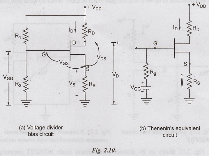
This
is because, in BJT, VBE = 0.7 V (silicon) with only minor variations
from one transistor to another But in a JFET, the VGs can vary several volts
from one JFET to another.
Electronic Devices and Circuits: Unit II: Amplifiers : Tag: : - Biasing the FET
Related Topics
Related Subjects

Electronic Devices and Circuits
EC3353 - EDC - 3rd Semester - ECE Dept - 2021 Regulation | 3rd Semester ECE Dept 2021 Regulation