Electronic Devices and Circuits: Unit I: Semiconductor Devices
Unijunction Transistor (UJT)
Construction, Operation
The UJT consists of a bar of lightly doped n-type silicon with a block of P-type material on one side
UNIJUNCTION TRANSISTOR (UJT)
UJT CONSTRUCTION AND OPERATION
The UJT consists of a bar of lightly doped n-type silicon with a block of P-type material on one side (Fig. 1.54 (a)). The end terminals of the bar are identified as base 1 (B1) and base 2 (B2) and the P-type block is named the emitter (E).
Fig.1.54
(b) shows the UJT equivalent circuit. The resistance of the n-type silicon bar
is represented as two resistors гB1 from B1 to point C,
and rB2 from B2 to C as illustrated. The sum of rB1
and rB2 is called RBB. The P type emitter forms a PN -
junction with the n-type silicon bar, and this junction is shown as a diode (D1)
in the equivalent circuit.

With
a voltage VB1B2 applied, the voltage at the junction point C is

Note
that V1 is also the voltage at the cathode of the diode in the
equivalent circuit with the emitter terminal open-circuited, the resistor
current is 
If
the terminal is grounded, the PN -junction is reverse biased and there is a
small emitter reverse current (IEO).
Now consider what happens when the emitter voltage (VEB1) is slowly increased from zero. When VEBI equals V1, the emitter current is zero. Further increase in VEBI forward-biases the PN-junctions and causes a forward current (IE) to flow from the p -type emitter into the n-type silicon bar. When this occurs, charge carriers are injected into the rB1 region. Since the resistance of the semiconductor material is dependent on doping, the additional charge carriers cause the resistance of the rB1 region to decrease rapidly. The decrease in resistance reduces the voltage drop across rB1 and so the pn junction in more heavily forward biased. This in turn results in a greater emitter current and more charge carriers that further reduce the resistance of the rB1 region. (The process is termed as regenerative).
The
input voltage is pulled down, and the emitter current (IE) is
increased to a limit deetrmined by the VEBI Source resistance. The
device remains in this on conditions until the emitter input is open-circuited
or until I is reduced to very low level.
The
circuit symbol for a UJT is shown in Fig. 1.54 (c). As always, the arowhead
points in the conventional current direction for a forward-biased junction. In
this case it points from the p-type emitter to n-type bar.
UJT CHARACTERISTICS
A
plot of emitter voltage VEBI versus emitter current IE gives the UJT
emitter characteristics. Refer to the UJT terminal voltage and currents shown
in Fig. 1.55 (a) and to the equivalent circuit Fig. 1.55 (b) Note that when VB1B2
= 0, IB2 = 0 and V1 =
0
If
VEB1 is now increased from zero, the resultant plot of VEB1
and IE is simply the characteristics of a forward-biased diode with
some series resistance. This is the characteristics for IB2 = 0 in
Fig. 1.55 (b).
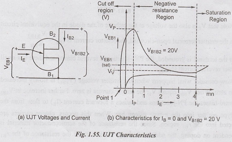
When
VB1B2 is 20 V, the level of V1 might be around 15 V1
depending on the resistance of rB1 and rB2. With VB1B2
= 20 V and VEBI = 0, the emitter junction is reverse-biased and the
emitter reverse current IEO flows as shown at point 1 on the VB1B2
= 20 V characteristic in Fig. 1.55 (b).
Increasing
VEBI until it equals V1 gives IE = 0. A
further increase in VEBI biases the emitter junction, and this gives
the peak point on the characteristic. At the peak point, VEBI is
identified as the peak voltage (VP) and Ie is termed the
peak current (IP).
Until
the peak point VP, the UJT is said to be operating in the cut off
region of its characteristics. When VEBI arrives at the peak
voltage, charge carriers are injected from the emitter to decrease the
resistance of rB1.
The
device enters the negative region, rB1 falls rapidly to a saturation
resistance (rS), and VEB1 falls to the valley voltage (VV).
IE also increases to the valley current (IV) at this time
increase in IE causes the device to enter the saturation region,
where the sum of Vd and IE X VS.
Electronic Devices and Circuits: Unit I: Semiconductor Devices : Tag: : Construction, Operation - Unijunction Transistor (UJT)
Related Topics
Related Subjects

Electronic Devices and Circuits
EC3353 - EDC - 3rd Semester - ECE Dept - 2021 Regulation | 3rd Semester ECE Dept 2021 Regulation