Electronic Devices and Circuits: Unit I: Semiconductor Devices
Types of Configuration
Common Base, Common Emitter, Common Collector | Configuration
When a transistor is to be connected in a circuit, one terminal is used as an input terminal, the other terminal is used as an output terminal and the third terminal is common to the input and output.
TYPES OF
CONFIGURATION
When
a transistor is to be connected in a circuit, one terminal is used as an input
terminal, the other terminal is used as an output terminal and the third
terminal is common to the input and output. Depending upon the input, output
and common terminal, a transistor can be connected in three configurations.
They are (i) Common Base (CB) Configuration (ii) Common Emitter (CE) and (iii)
Common Collector (CC) Configuration.
Common Base Configuration
This
is also called grounded base configuration. In this configuration, emitter is
the input terminal, collector is the output terminal and base is the common
terminal.
The circuit for determining the static characteristics curve of an NPN transistor in the common base configuration is shown in Fig.1.37.

Input Characteristics
To determine the input characteristics, the collector base voltage VCB is kept constant at zero volt and the emitter current IE is increased from zero in suitable equal steps by increasing VEB. This is repreated for higher fixed values of VCB. A curve is drawn between emitter current IB and emitter-base voltage VEB at constant collector-base voltage VCB. The input chracteristics thus obtained are shown in Fig. 1.38.
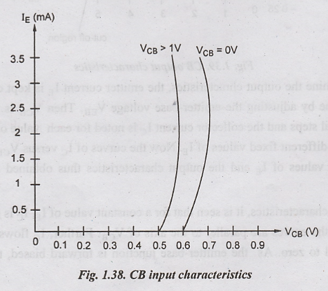
When
VCB is equal to zero and the emitter-base junction is forward biased
as shown in the characteristics. The junction behaves as a forward biased diode
so that emitter current IE increases rapidly with small increase in
emitter-base voltage VEB
When
VCB is increased keeping VEB constant, the width of the
base region will decrease. This effect results in an increase of IE.
Therefore, the curves shift towards the left as VCB is increased.
Output Characteristics

To
determine the output characteristics, the emitter current IE is kept
constant at a suitable value by adjusting the emitter-base voltage VEB.
Then VCB is increased in suitable equal steps and the collector
current IC is noted for each value of IE. This is repeated
for different fixed values of IE. Now the curves of IC
versus VCB are plotted for constant values of IE and the
output characteristics thus obtained is shown in Fig. 1.39.
From the characteristics, it is seen that for a constant value of IE, IC is independent of VCB and the curves are parallel to the axis of VCB. Further, IC flows even when VCB is equal to zero. As the emitter-base junction is forward biased, the majority
carriers
i.e., electrons from the emitter are injected into the base region. Due to the
action of the internal potential barrier at the reverse baised collector-base
junction, they flow to the collector region and give rise to IC even
when VCB is equal to zero.
(i)
Input Impedance (hib)
It
is defined as the ratio of the change in (input) emitter voltage to the change
in (input) emitter current with the (output) collector voltage VCB
kept constant. Therefore,

It
is the slope of CB input characteristics IE versus VEB as
shown in Fig. 1.38. The typical value of hit ranges from 20 to 50 Ω.
(ii)
Output Admittance (hob)
It
is defined as the ratio of the change in (output) collector current to the
corresponding change in the (output) collector voltage with the (input) emitter
current IE kept constant. Therefore,

It
is the slope of CB output characteristics IC versus VCB
as shown in Fig. 1.39. The typical value of the parameter is of the order of
0.1 to 10 μhos.
(iii)
Forward Current Gain (hfb)
It
is detected as a ratio of the change in the (output) collector current to the
corresponding change in the (input) emitter current keeping the (output)
collector voltage VCB constant. Hence,
It
is the slope of IC versus IE curve. Its typical value
varies from 0.9 to 1.0.
(iv)
Reverse Voltage Gain (hrb)
It is defined as the ratio of the change in the (input) emitter voltage and the corresponding change in (output) collector voltage with constant (input)emitter current, IE. Hence,

It
is the slope of VEB Vs VCB curve. Its typical value is
the order of 10-5 to 10-4.
Common Emitter Configuration
Input Characteristics
To
determine the input characteristics the collector to emitter voltage is kept
constant at zero volt and base current is increased from zero in equal steps by
increasing VBE in the circuit shown in Fig. 1.40.
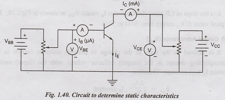
The
value of VBE is noted for each settling of IB. This
procedure is repeated for higher fixed values of VCE, and the curves
of IB Vs VBE are drawn. The input characteristics thus
obtained are shown in Fig. 1.41.

When
VCE = 0, the emitter base junction is forward biased and the
junction behaves as a forward biased diode.
Hence
the input characteristics for VCE = 0 is similar to that of a
forward biased diode. When VCE is increased the width of the
depletion region at the reverse biased collector base junction will increase.
Hence the effective width of the base will decrease. This effect causes a
decrease in the base current IB. Hence to get the same value of Ib
as that for VCE = 0, VBE should be increased. Therefore,
the curve shifts to the right as VCE increases.
Output Characteristics
To
determine the output characteristics, the base current IB is kept
constant at a suitable value by adjusting base-emitter voltage, VBE.
The magnitude of collector- emitter voltage VCE is increased in
suitable equal steps from zero and the collector current IC is noted
for each setting VCE. Now the curves of IC versus VCE
are plotted for different constant values of IB. The output
characteristics are obtained shown in Fig. 1.42.
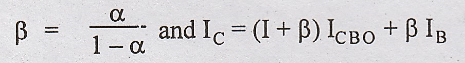
For
larger values of VCE, due to Early effect, a very small change in a
is reflected in a very large change in β.
The
output characteristics of CE configuration show a larger slope when compared
with CB configuration.
The
output characteristics have three regions namely, saturation region, cutoff
region and active region.
The
region of curves to the left of the line OA is called the saturation region,
and the line OA is called the saturation line. In this region, both junctions
are forward biased and an increase in the base current does not cause a
corresponding large change in IC. The ratio of VCE(sat)
to IC in this region is called saturation resistance.
The region below the curve for IB = 0 is called the cut-off region. In this region, both junctions are reverse biased. When the operating point for the transistor enters the cutoff region, the transistor is OFF. Hence the collector current becomes almost
zero
and the collector voltage almost equals VCC, the collector supply
voltage. The transistor is virtually an open circuit between collector and
emitter.

The
central region where the curves are uniform in spacing and slope is called the
active region. In this region, emitter-base junction is forward biased and the
collector base junction is reverse biased. If the transistor is to be used as a
linear amplifier it should be operated in the active region.
Transistor Parameters
The
slope of the CE characteristics will give the following four transistor
parameters. Since these parameters have different dimensions, they are commonly
known as common emitter hybrid parameters or h-parameters.
(i)
Output Admittance (hoe)
It
is defined as the ratio of change in the (output) collector current to the
corresponding change in the (output) collector voltage with the (input) base
current IB kept constant. Therefore
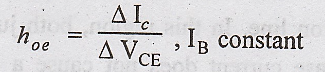
It
is the slope of CE output characteristic IC Vs VCE. The
typical value of this parameter is of the order of 0.1 to 10 μ mhos.
(ii)
Input Impedance (hie)
It
is defined as the ratio of the change in (input) base voltage to the change in
(input) base current with the (output) collector voltage VCE kept
constant.

It
is the slope of CE input characteristics IB versus VBE,
the typical value of hie ranges from 500 to 2000 Ω.
(iii)
Forward Current Gain (hfe)
It
is defined as a ratio of the change in the (output) collector current to the
corresponding change in the (input) base current keeping the (output) collector
voltage VCE constant. Hence
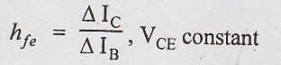
It
is the slope of IC versus IB curve. Its typical value
varies from 20 to 200.
(iv)
Reverse Voltage Gain (hre)
It
is defined as the ratio of the change in the (input) base voltage and the
corresponding change in (output) collector voltage with constant (input) base
current, IB. Hence,

It
is the slope of VBE Versus VCE curve. Its typical value
is of the order of 10-5 to 10-4.
Common Collector Configuration

The
circuit diagram for determining the static characteristics of an NPN transistor
in the common collector configuration is shown in Fig. 1.43.
Input Characteristics
To
determine the input characteristics, VEC is kept at a suitable fixed
value. The base-collector voltage VBC is increased in equal steps
and the corresponding increase in IB is noted. This is repeated for
different fixed values of VEC. Plots of VBC versus IB
for different values of VEC shown in Fig. 1.44 are the input
characteristics.

Output Characteristics

The
output characteristics shown in Fig. 1.45 are same as those of the common
emitter configuration.
Electronic Devices and Circuits: Unit I: Semiconductor Devices : Tag: : Common Base, Common Emitter, Common Collector | Configuration - Types of Configuration
Related Topics
Related Subjects

Electronic Devices and Circuits
EC3353 - EDC - 3rd Semester - ECE Dept - 2021 Regulation | 3rd Semester ECE Dept 2021 Regulation