Electronic Devices and Circuits: Unit I: Semiconductor Devices
Transition or Space Charge or Depletion Capacitance
Derivation
When PN diode is reverse biased, the majority charge carriers move away from the junction and large immobile carriers are generated near the junction. The width of the space - charge layer increases with increasing reverse voltage.
TRANSITION OR SPACE CHARGE OR DEPLETION CAPACITANCE
When
PN diode is reverse biased, the majority charge carriers move away from the
junction and large immobile carriers are generated near the junction. The width
of the space - charge layer increases with increasing reverse voltage.
Thus
the increase in uncovered charge with applied voltage is considered as a
capacitor. The two parallel layers of oppositely charged immobile ions form the
two plates of capacitor, CT.
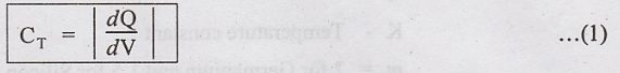
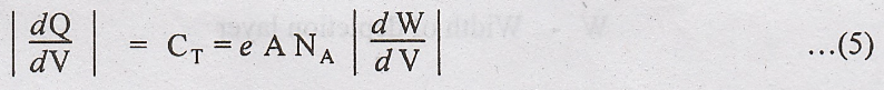
Where
dQ/dv - change in charge due to change in voltage
The
change in voltage dV in a time dt results in current
I
= dQ/dt .................(2)
(1)
can be written as
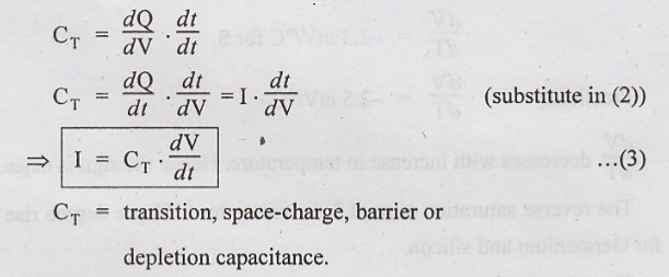
CT
= transition, space-charge, barrier or depletion capacitance.
CT
is derived for two cases
i.
Step-graded junction
ii.
Linearly graded junction
i. Step Graded Junction
A
PN junction is formed from a single intrinsic semiconductor by doping part of
it with acceptor impurities and the remaining with donors.
There
is a sudden step change from acceptor ions on one side to donor ions on the
other side. Trivalent Indium is placed against N-type germanium and heated to
high temperature.
Some of the Indium dissolves into the Germanium and N-type Germanium is changed to P-type at the junction. This step-graded junction is called an alloy or fusion junction.
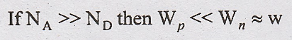
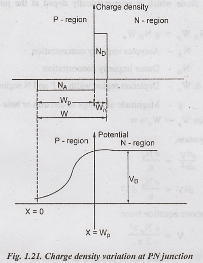
Consider
a PN diode which is asymmetrically doped at the junction. The net charge is
zero,
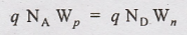
Where
NA - Acceptor impurity concentration
ND
- Donor impurity concentration
Wp
& Wn - Depletion region width of P and N region
q
- Magnitude of charge of electron or hole
By
poisson's equation,
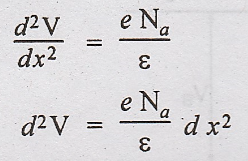
Integrating
the above equation twice
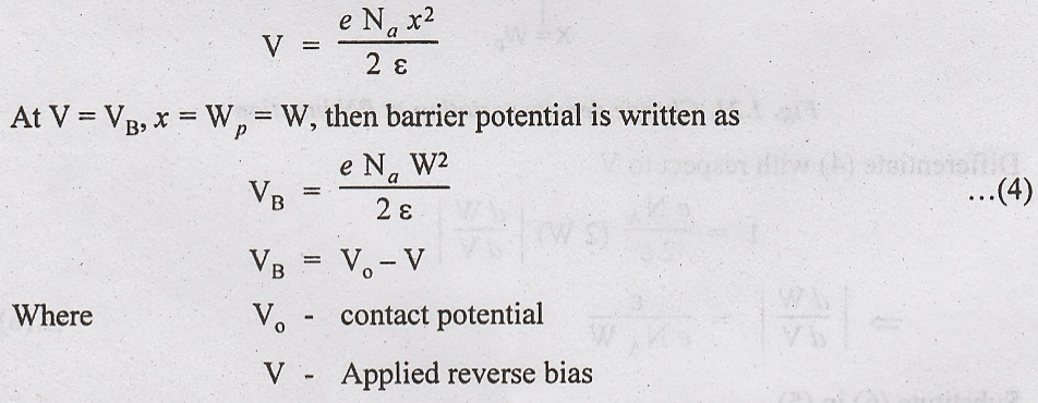
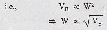
Width
of depletion layer, W increases with applied reverse voltage
Total
charge density of P-type material
Differentiate
above equation with respect to V
Differentiate
(4) with respect to V
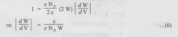
Substitute
(6) in (5)
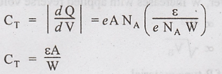
Where
ε
- permittivity of the material
A
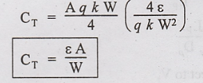
- Cross sectional area of the junction
W - Width of depletion layer
The
depletion width W is given by
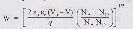
When
no external voltage is applied, width of PN diode is of the order of 0.5
microns. The majority carriers move across the junction and opposite charges
are stored at a distance W apart. This depletion region acts as dielectric
between P and N regions. Thus it acts as a parallel plate capacitor with
transition capacitance CT approximately 20 PF with no external bias.
CT ranges from 5 to 200 PF with applied voltage.
ii. Linearly Graded Junction
The
charge density varies linearly with the applied voltage.
Linear
graded junction is formed by melting Germanium and its type is changed during
the drawing process by adding first p-type and then n-type impurities. The
charge density becomes absolutely zero at edge distances and W/2 W/2 and varies
linearly with distance.

Where
k - proportionality constant
Using
Poisson's equation

Where
V - potential at a distance 'x' from the junction
Integrating
(2)
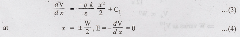
Substitute
(4) in (3)

Substitute (5) in (3)
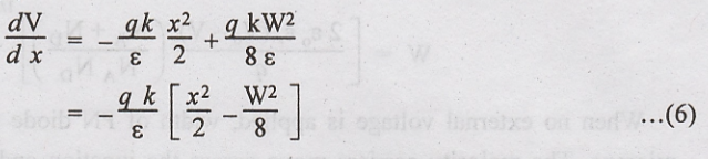
Integrating
(6)
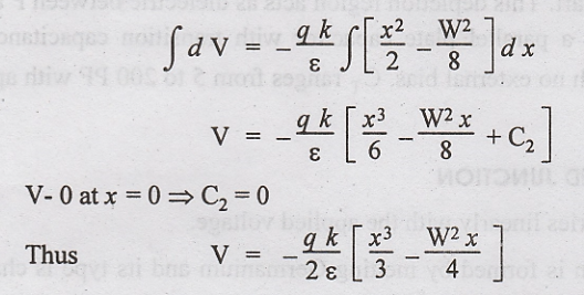
The
total potential VJ across the junction from - W/2 to W/2 is given by
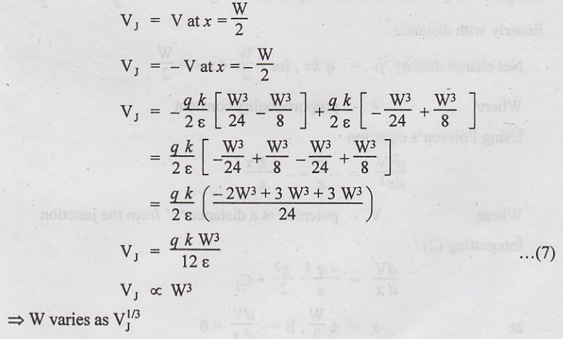
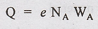
The
total charge on one side of the layer is
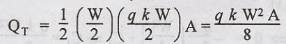
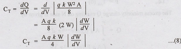
From
(7)
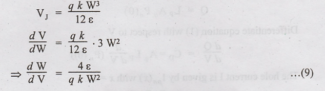
Substitute
(9) in (8)
Electronic Devices and Circuits: Unit I: Semiconductor Devices : Tag: : Derivation - Transition or Space Charge or Depletion Capacitance
Related Topics
Related Subjects

Electronic Devices and Circuits
EC3353 - EDC - 3rd Semester - ECE Dept - 2021 Regulation | 3rd Semester ECE Dept 2021 Regulation