Physics for Electronics Engineering: Unit V: Nano Devices
Quantum Resistance and Conductance
Schematic Diagram, Formula, Derivation
For an elementary description of quantum conductance effects, it is more appropriate to deal with 1D mesoscopic semiconductor structures like quantum wires.
QUANTUM RESISTANCE AND CONDUCTANCE
For
an elementary description of quantum conductance effects, it is more
appropriate to deal with 1D mesoscopic semiconductor structures like quantum
wires.
If
the wire is short enough, ie., shorter than the electron mean free path in the material,
there will be no scattering and the transport is ballistic.
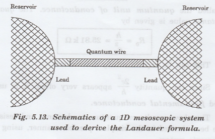
As
in fig. 5.13, the 1D quantum wire is connected through ideal leads. They do not
produce scattering events to reservoirs characterized by Fermi levels EF1
and EF2:
In
order to flow of the current through the quantum wire, a small voltage V is
applied between the reservoirs.
As
a consequence, there is a potential energy eV between the two reservoirs equal
to EF1 - EF2. The current across the wire should be given
by the product of the concentration of electrons (obtained from the density of
states function n1D(E), in the energy interval (eV), the electron
velocity v (E), and the unit
electronic charge:

Substituting
for n1D(E) by its expression, we obtain the following value of the current:
It
is independent of the carrier velocity.
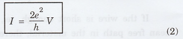
The
value of the conductance G = (I/V) is therefore:

It
is interesting to observe that the conductance of the quantum wire is length independent,
in contrast to the classical case where it varies inversely to the length.
The
quotient
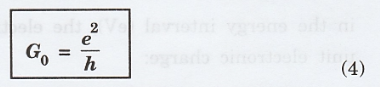
is
called the quantum unit of conductance. The quantum resistance value is given
by
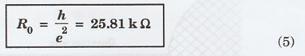
This
can be experimentally determined.
Since
the quantity 2e2/h appears very often, it is usually called
fundamental conductance.
The above results on quantum conductance and resistance have been derived in the simplest possible manner, using a 1D mesoscopic system.
This
quantification of macroscopic classical concepts, like conductance and resistance,
is of fundamental importance in mesoscopic physics.
Carbon
In
nanotechnology, researchers are looking out for certain materials with desired properties
through which the nanoscale components and structures can be obtained.
Carbon
is found to be one such material suitable for nano- technology based components
due to its inherent desirable properties.
Carbon
is a unique atom among other elements because of its ability to exist in a wide
variety of structures and forms as shown in the fig. 5.14.
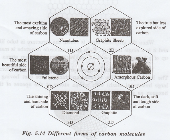
Pure carbon exists in four different crystalline forms namely Diamond, Graphite, Fullerenes and Nanotubes.
Carbon
atom is the basic building block of these crystalline structure. Among these, Fullerenes
and Nanotubes are found to be useful in nanotechnology for various
fabrication
of nanostructures.
Physics for Electronics Engineering: Unit V: Nano Devices : Tag: : Schematic Diagram, Formula, Derivation - Quantum Resistance and Conductance
Related Topics
Related Subjects

Physics for Electronics Engineering
PH3254 - Physics II - 2nd Semester - ECE Department - 2021 Regulation | 2nd Semester ECE Dept 2021 Regulation