Electronic Devices and Circuits: Unit V: Power Amplifiers and DC/DC Converters
Power MOSFET
Construction, Operation, Characteristics
Power MOSFET is a special type of MOSFET designed to handle high power levels. Power MOSFET are commonly used power devices due to the following advantages. 1. Low gate drive power 2. Fast switching speed 3. Parallel operation
POWER MOSFET
Power
MOSFET is a special type of MOSFET designed to handle high power levels.
Power
MOSFET are commonly used power devices due to the following advantages.
1.
Low gate drive power
2.
Fast switching speed
3.
Parallel operation
For
high power applications, the standards MOSFET structure cannot be used because
1. To increase current capability of MOSFET, its width should be made large and its channel length L should be made as small as possible. But it reduces the breakdown voltage and can't handle high voltages in power transistor applications.
Therefore,
MOSFET is designed with short channel fabrication (1 to 2 μm) with high
breakdown voltages.
CONSTRUCTION
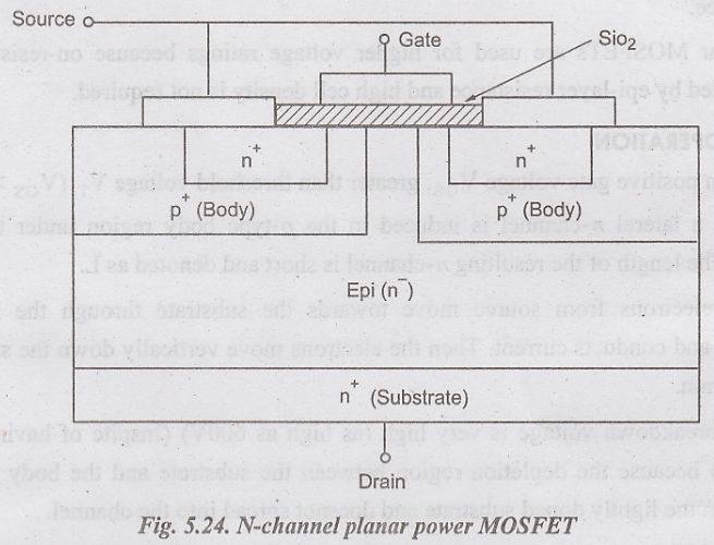
Double-diffused
MOSFET (or) DMOS transistor is used as power MOSFET. The device is fabricated
on a lightly doped n-type substrate with a heavily doped region at the bottom
for the drain contact. Two diffusions are used one to form p-type body region
and other to form the n-type source region.
In
power MOSFETs, source and drain are constructed on opposite sides of a vertical
structure in order to support higher current and voltage. The structure of
power MOSFET is classified into horizontal and vertical type. Vertical type is
further classified into planar type and trench type.

In
vertical power MOSFET, the current flows in the vertical direction, the on-
resistance per chip area is reduced due to miniaturization. Trench MOSFETs are
used for voltage rating of < 200 V due to their higher channel density and
lower on- resistance.
Planar
MOSFETs are used for higher voltage ratings because on-resistance is dominated
by epi-layer resistance and high cell density is not required.
OPERATION
When
positive gate voltage VGS, greater than threshold voltage VT (VGS
> VT) is applied, a lateral n-channel is induced in the p-type
body region under the gate oxide. The length of the resulting n-channel is
short and denoted as L.
The
electrons from source move towards the substrate through the induced channel
and conducts current. Then the electrons move vertically down the substrate to
the drain.
The
breakdown voltage is very high (as high as 600V) (Inspite of having short
channel) because the depletion region between the substrate and the body
extends mostly in the lightly doped substrate and doesnot spread into the
channel.
Thus MOS transistor has a high current capability (≈ 50A) and high breakdown voltage. The vertical structure of the device enables efficient utilization of the silicon area.
CHARACTERISTICS
Power
MOSFETs has threshold voltages in the range of 2V to 4V. The drain current and
VGS are related by

The
high electric field in the short channel increases the velocity of charge
carriers to be maximum. This is known as velocity saturation. Thus the drain
current is given by
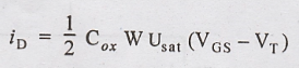
where Usat → Saturation velocity (5 x 106 cm/s for electrons in Silicon)
The
linear iD - VGS relationship implies a constant gm
in the velocity – saturation region.
gm
is proportional to W and is large for power devices. Thus, power MOSFETs have
high transconductance values.

Electronic Devices and Circuits: Unit V: Power Amplifiers and DC/DC Converters : Tag: : Construction, Operation, Characteristics - Power MOSFET
Related Topics
Related Subjects

Electronic Devices and Circuits
EC3353 - EDC - 3rd Semester - ECE Dept - 2021 Regulation | 3rd Semester ECE Dept 2021 Regulation