Electronic Devices and Circuits: Unit I: Semiconductor Devices
PN Diode
N Type material, Operation of a PN Junction mode
In a piece of semiconductor, one half is doped by P-type impurity and the other half is doped by N-type impurity. Thus PN junction is formed.
PN DIODE
i.
In a piece of semiconductor, one half is doped by P-type impurity and the other
half is doped by N-type impurity. Thus PN junction is formed.
ii.
This formation of PN junction is called diode as it has two electrodes one for
P region called as Anode and the other for N region called as Cathode.
N-Type Material
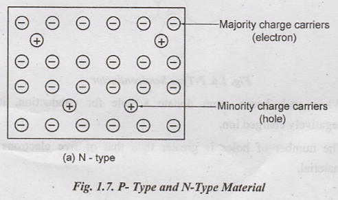
The
majority charge carriers are electrons and has higher concentration of free
electrons than holes as shown in Fig.1.7 (a).
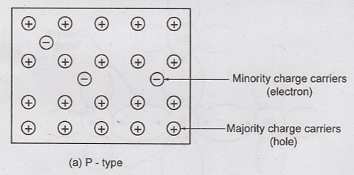
The
majority charge carriers are holes and P type material has higher concentration
of holes than electrons, as shown in Fig. 1.7 (b).
Diffusion
The
tendency of the free electrons to diffuse from the n-side to p-side and holes
from p- region to n-region is called diffusion.
Diffusion
is the process by which charge carrier moves from high concentration region to
low concentration region.
Depletion Region
The
free electrons diffuse from 'n' side to 'p' side region and recombine with the
holes in P region. Thus negative charged immobile ions are formed near the junction.
Also,
the holes diffuse from P-region to n-region and recombine with the electrons in
n-region and leaves positively charged immobile ions near the junction of
n-side.
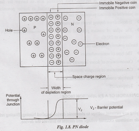
This
process continues over certain time duration. After certain extent, the net
negative charge on P-side prevents further diffusion of electrons into P-side.
Similarly, the net positive charge on N-side repels holes crossing from P-side
to N- side. These immobile positive and negative ions form a region called as depletion
region.
Depletion
region is defined as the region over which all the free charge carriers are
depleted. This region is also known as space charge region since there are no
free charge carriers available for conduction. In equilibrium condition, the
depletion region gets widened upto a point where no further electrons or holes
can cross the junction. The physical distance from one side to other side of
the depletion region is called width of the depletion region.
Barrier Potential
The
electric filed is developed across the depletion region due to the potential
difference between P and N regions. This potential acts as barrier for further
conduction between the junction. This potential is called as barrier potential
or diffusion potential or contact potential or cut in voltage.
i.
It depends on doping levels and temperature
ii.
The value of contact potential is 0.3 V for Germanium and 0.72V for Silicon at
25° C.
The
barrier potential depends on
i.
The type of semiconductors
ii.
Concentration of donor impurity on n- side
iii.
Concentration of acceptor impurity on p - side
iv.
Intrinsic concentration of semiconductors
v.
Temperature ܀
OPERATION OF A PN JUNCTION DIODE
Biasing
Applying any external voltage to electronic device is called biasing. Biasing refers to provide minimum external voltage and current to activate the device.
There
are two types of biasing for PN junction.
Forward Bias
The
positive terminal of the battery is connected to P-type semiconductor and
negative terminal is connected to n-type semiconductor material.
Reverse Bias
The
positive terminal of the battery is connected to n - type semiconductor and the
negative terminal is connected to P-type semiconductor material.
Electronic Devices and Circuits: Unit I: Semiconductor Devices : Tag: : N Type material, Operation of a PN Junction mode - PN Diode
Related Topics
Related Subjects

Electronic Devices and Circuits
EC3353 - EDC - 3rd Semester - ECE Dept - 2021 Regulation | 3rd Semester ECE Dept 2021 Regulation