Electronic Devices and Circuits: Unit I: Semiconductor Devices
Metal Oxide Semiconductor Field Effect Transistor (MOSFET)
Semiconductor Devices
MOSFET is the common term for the Insulated Gate Field Effect Transistor (IGFET). There are two basic terms of MOSFET (i) Enhancement MOSFET and (ii) Depletion MOSFET.
METAL OXIDE SEMICONDUCTOR FIELD EFFECT TRANSISTOR (MOSFET)
MOSFET
is the common term for the Insulated Gate Field Effect Transistor (IGFET).
There are two basic terms of MOSFET (i) Enhancement MOSFET and (ii) Depletion
MOSFET.
Principle
By
applying a transverse electric field across an insulator, deposited on the
semiconducting material, the thickness and hence the resistance of a conducting
channel of a semiconducting material can be controlled.
In
a depletion MOSFET, the controlling electric field reduces the number of
majority carriers available for conduction, whereas in the enhancement MOSFET,
application of electric field causes an increase in the majority carrier
density in the conducting regions of the transistor.
ENHANCEMENT MOSFET
Construction
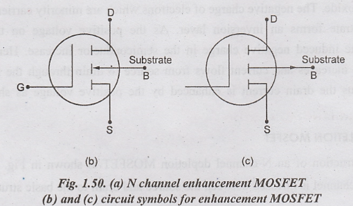
The construction of an N-channel enhancement MOSFET is shown in Fig. 1,50(a) and the circuit symbols for an N-channel and a P-channel enhancement MOSFET are shown in Fig. 1.50 (b) and 1.50(c) respectively. As there is no continuous channel in an enhancement MOSFET, this condition is represented by the broken line in the symbols.
Two
highly doped N+ regions are diffused in a lightly doped substrate of P-type
silicon substrate. One N+ region is called the source S and the other one is
called the drain D. They are seperated by 1 mil (10-3 inch). A thin insulating
layer of SiO2 is grown over the surface of the structure of SiO2
is grown over the surface of the structure and holes are cut into the oxide
layer, allowing contact with source and drain. Then a thin layer of metal
aluminium is formed over the layer of SiO2. This metal layer covers
the entire channel region and it forms the gate G.
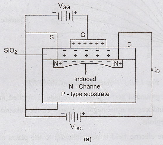
The metal area of the gate, in conjunction with the insulating oxide layer of SiO2 and the semiconductor channel forms a parallel plate capacitor. This device is called the insulated gate FET because of the insulating layer of SiO2. This layer gives an extremely high input impedance for the MOSFET.
Operation

If
the substrate is grounded and a positive voltage is applied at the gate, the
positive charge on G induces an equal negative charge on the substrate side
between the source and drain regions.
The
direction of the electric field is perpendicular to the plates of the capacitor
through the oxide. The negative charge of electrons which are minority carriers
in the P-type substrate forms an inversion layer. As the positive voltage on
the gate increases, the induced negative charge in the semiconductor increase.
Hence, the conductivity increases and current flows from source to drain
through the induced channel. Thus the drain current is enhanced by the positive
voltage as shown in Fig. 1.51.
DEPLETION MOSFET
The
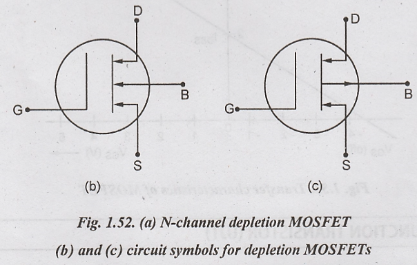
construction of an N-channel depletion MOSFET is shown in Fig. 1.52(a) where an
N channel is diffused between the source and drain to the basic structure of
MOSFET.
The circuit symbols for an N-channel and a P-channel depletion MOSFET are shown in Fig. 1.52 (b) and 1.52 (c) respectively.
With
VGS = 0 and the drain D at a positive potential with respect to the
source, the electrons (majority carriers) flow through the channel D to S. If
the gate voltage is made negative, positive charge consisting of holes is induced
in the channel through SiO2 of the gate channel capacitor. The
introduction of the positive charge causes depletion of mobile electrons on the
channel.

Thus a depletion region is produced in the channel. The shape of the depletion region depends on VGS and VDS. Hence the channel will be wedge shaped as shown in Fig.1.52. When VDS increased, ID increases and it becomes practically constant at a certain value of VDS, called the Pinch-Off voltage. The drain current ID almost gets saturated beyond the pinch-off voltage.
Since
the current in an FET is due to majority carriers (electrons for an N-type
material) the induced positive charges make the channel less conductive, and ID
drops as VGS is made negative.
The
depletion MOSFET may also be operated in an enhancement mode. It is only
necessary to apply a positive gate voltage so that negative charges are induced
into the N-type channel. Hence the conductivity of the channel increases and ID
increases. As the depletion MOSFET can be operated with bipolar input signals
irrespective of doping of the channel, it is also called as dual mode MOSFET.
The volt ampere characteristics are induced in Fig. 1.51.
The
curve of ID versus VGS for constant VDS for is
called the transfer characteristics of MOSFET and is shown in Fig. 1.53.

Electronic Devices and Circuits: Unit I: Semiconductor Devices : Tag: : Semiconductor Devices - Metal Oxide Semiconductor Field Effect Transistor (MOSFET)
Related Topics
Related Subjects

Electronic Devices and Circuits
EC3353 - EDC - 3rd Semester - ECE Dept - 2021 Regulation | 3rd Semester ECE Dept 2021 Regulation