Electronic Devices and Circuits: Unit I: Semiconductor Devices
Introduction of Semiconductor Devices
Energy Band Theory - Energy Band Diagram - Semiconductor Devices
An electronic device is essentially a device in which electrons flow through a vacuum or gas or semiconductor. An atom is composed of charged particles namely electrons and protons.
SEMICONDUCTOR DEVICES
INTRODUCTION
An
electronic device is essentially a device in which electrons flow through a
vacuum or gas or semiconductor. An atom is composed of charged particles namely
electrons and protons. The nucleus consists of a number of neutral particles
called neutrons and a number of positively charged called protons. The electron
spirals towards the nucleus and when an electron jumps from higher orbits to
lower orbits, the radiation of energy takes place. The electrons in the innermost
shells are very strongly attached to the atom and have the minimum energy.
Hence, these electrons cannot be easily separated.
ENERGY-BAND THEORY
An
electron revolving around the nucleus of an atom has potential energy, boller
centrifugal energy, magnetic energy and rotational energy. These energies
determine the total energy or energy level of an electron, measured as electron
volt.
An
electron volt can be defined as the amount of energy required to move an
electron through a potential of one volt i.e., the amount of energy gained or
lost when an electron falls through or moves against the potential difference
of one volt.
1 eV = 1.6 x 10⁻¹⁹
Joules
Each
shell has an energy level. An electron in the outermost orbit is loosely bound
to the nucleus and has higher energy. Similarly, the electron revolving in the
inner shell very close to the nucleus is very tightly bound and has only a
small amount of energy. Thus, it cannot be easily isolated from an individual
atom.
Hence,
the valence electrons in the outermost shell can be easily extracted from the
atom. These isolated electrons involve in chemical reactions and bond the atoms
together.
Covalent Bond
The
valence electrons form a bond with the valence electrons of an adjacent atom.
This bond is called covalent bond.
Energy Band
The
valence electrons having highest energy level form the covalent bonds. The
energy levels of the corresponding valence electrons merge into each other due
to the coupling between valence electron. This creates an energy band i.e.,
closely spaced energy levels.
Energy-Gap
The
difference between the energy levels of any orbits is called as energy gap.
In
practice, only two bands of energy levels are considered. They are valence band
and conduction band.
Valence Band
The
valence electrons combine together to form the covalent bonds. The energy band
formed due to merging of energy levels related with the free electrons is
called valence band.
Conduction Band
When
energy is applied to the valence electrons in the covalent bond, these valence
electrons escape from the bond and the electrons become free to conduct. The
energy band due to merging of energy levels associated with the free electrons
is called conduction band.
Forbidden Energy Gap
The energy gap between the conduction band and the valence band is called forbidden energy gap.
ENERGY BAND DIAGRAM
The
graphical representation of the energy bands in a solid is called energy band
diagram.
The
materials are classified into three types depending on the energy band diagram.
Insulator
In
insulator, the forbidden energy gap is very large between the conduction band
and the valence band. Hence large electric field is required to remove the
electrons from valence band to conduction band. Practically, it is impossible
for an electron to jump from valence band to conduction band. The number of
free electrons in the insulator is very small in the order of 107 electrons/m3.
The forbidden energy gap is very large about 7 eV. For example, in diamond, the
energy gap is 6 eV. Fig. 1.1 shows the energy band diagram of an insulator.
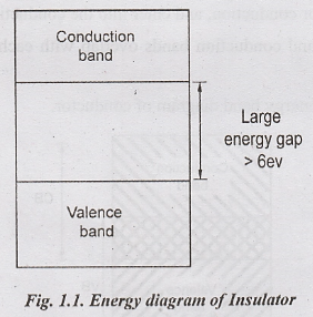
In
general, Insulator has
i.
Full valence band
ii.
Empty conduction band
iii.
Large energy gap
iv. Negative temperature co-efficient i.e when temperature is increased some valence band electrons acquire energy and moves to the conduction band.
Properties
i.
Conductivity is poor
ii.
Rigid, crystalline nature
iii.
High melting and boiling temperature
iv.
Unidirectional
Conductors
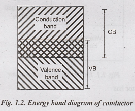
A
conductor is a material that easily conduct or pas the current. In conductor,
the valence band and conduction band, overlap together. Example: copper,
silver, gold, Aluminium.
The
atoms of the above material consists of only one valence electron which is
loosely bound to the atom.
These
valence electrons can be easily broken away from their atom and become free
electrons ready for conduction, and enter into the conduction band.
Thus
the valence and conduction bands overlap with each other and there is no
forbidden energy gap.
Fig.1.2
shows the energy band diagram of conductor.
Properties
i.
Good Conductivity
ii.
Rigid, crystalline nature
iii.
Low melting and boiling temperature
iv. Non-directional
Semiconductor
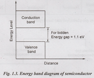
Semiconductor
is a material whose electrical properties lies in between that of insulators
and conductors.
They
have partially filled conduction band and valence band with narrow energy
between the two bands, Ex. Silicon, Germanium, Gallium Arsenide etc.
At
OK there are no electrons in the conduction band and the valence band is
completely filled. Thus it behaves as an insulator.
When
the temperature is increased, some of the electrons in the valence band enter
into the conduction band. Thus it behaves as conductor.
The
electrical conductivity of the semiconductor lies in the range of 10-3 to 10-6
per ohm per cm.
Fig.1.3
shows the energy band diagram of semiconductors.
Properties
i.
Conductivity can be increased by doping.
ii.
Low melting and boiling temperature.
iii.
Rigid, crystalline nature.
iv.
Directional.
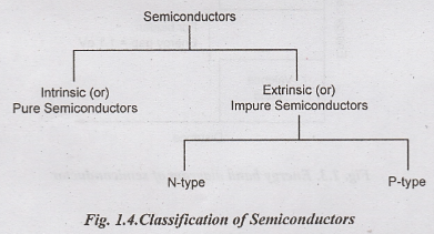
Semiconductors
are classified into two types
Electronic Devices and Circuits: Unit I: Semiconductor Devices : Tag: : Energy Band Theory - Energy Band Diagram - Semiconductor Devices - Introduction of Semiconductor Devices
Related Topics
Related Subjects

Electronic Devices and Circuits
EC3353 - EDC - 3rd Semester - ECE Dept - 2021 Regulation | 3rd Semester ECE Dept 2021 Regulation