Electronic Devices and Circuits: Unit I: Semiconductor Devices
Important Two Marks Questions with Answers on Semiconductor Devices
Anna University Important Two mark and Review questions in Semiconductor Devices
TWO MARKS QUESTION AND ANSWERS
1.
What is meant by valence electron?
The
electrons in the outermost shell of an atom is called vallence electron.
2.
Define forbidden energy gap.
The
space between the valence band and conduction band is energy gap.
3.
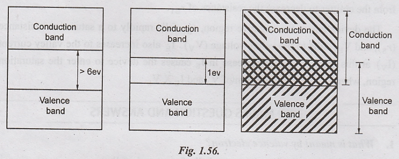
What are conductors?
Conductors
are materials in which valence and conduction band overlap with each other.
Example:
Copper, Silver
4.
What do you mean by insulator?
Insulator
is a material in which the valence and conduction band are far away from each
other. The energy gap between the valence and conduction band is larger.
Example:
Glass, Plastic
5.
What is meant by semiconductor?
The
material whose electrical property lies between that of conductors and
insulator is called semiconductor.
Example:
Silicon, Germanium
6.
Define mass-action law.
Under
thermal equilibrium the product of free electron concentration and hole
concentration is constant regardless of the individual magnitude
7.
Draw the Energy band diagram of conductors, semiconductors and Insulators.
8.
Define intrinsic semiconductor.
The
semiconductor in its purest form is called intrinsic semiconductor.
9.
Define Extrinsic semiconductor.
If
certain amount of impurity is added to intrinsic semiconductor then the
resulting semiconductors is called Extrinsic semiconductor.
10.
What are the types of Extrinsic semiconductor.
i.
P-type semiconductor
ii.
N-type semiconductor.
11.
What is P-type semiconductor?
The
semiconductor which is obtained by adding pentavalent impurity atom to an
intrinsic semiconductor is called as P-type semiconductor.
Ex:
Phosphorous, Antimony are pentavalent impurities
12.
What is N-type semiconductor?
The
semiconductor which is obtained by introducing trivalent impurity atom
(Gallium, Indium) is called N-type semiconductor.
13.
Define doping.
The
process of adding impurity to an intrinsic semiconductor is called doping. The
impurity is called dopant.
14.
What is P-type semiconductor?
In
P-type semiconductor, the majority charge carriers are holes and the minority
charge carriers are electrons.
15.
What is N-type semiconductor?
In
N-type semiconductor, the majority charge carriers are electrons and the
minority charge carriers are holes.
16.
What is donor impurity?
Pentavalent
impurity will donate the excess negative charge carriers (electrons) and hence,
n-type or pentavalent impurity is called as donor impurity.
17.
Why P-type or trivalent impurity is called acceptor impurity?
P-type
impurity creates holes which can accept electron. So, these impurities are
called acceptor impurities.
18.
How PN diode is formed?
If
a semiconductor is doped with P-type impurity on one half side and N-type
impurity on other half side, then the semiconductor is called PN diode.
19.
Define biasing.
Biasing
is defined as the application of any external voltage to an electronic device.
20.
What are the types of bias?
i.
Forward bias
ii.
Reverse bias
21.
What is meant by forward bias?
The
positive terminal of the battery is connected to P-type semiconductor and
negative terminal is connected to n-type semiconductor.
22.
What is meant by reverse bias.
The
positive terminal of the battery is connected to n-type and negative terminal
is connected to p-type semiconductor.
23.
What is depletion region?
The
region around the junction from which the mobile charge carriers (electrons and
holes) are depleted is called depletion region.
It
is also called space charge region because this region has electrically bd
charged immobile ions.
24.
Draw the V-I characteristics of PN diode.
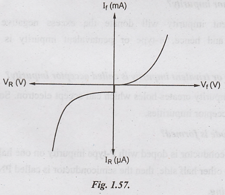
25.
What is barrier potential?
The
oppositely charged ions in both sides of PN junction creates an electric
potential across the junction. This is called barrier potential.
26.
Define reverse saturation current.
The
current due to the minority carriers in reverse bias is called reverse
saturation current.
27.
Define forward resistance.
The
resistance offered by the p-n junction diode in forward biased condition is
called forward resistance.
28.
What are the types of forward resistance?
i.
Static or dc resistance
ii.
Dynamic or ac resistance
29.
Define reverse resistance.
Reverse
resistance is defined as the resistance offered by the PN junction diode under
reverse bias condition.
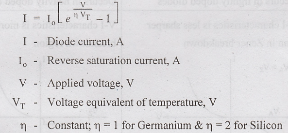
30.
Write the diode current equation.
31.
What are the breakdown mechanisms in PN diode?
i.
Avalanche breakdown
ii
Zener breakdown
32.
Define Fermilevel.
Fermilevel
is defined as that energy level where the probability of occupation of charged
carrier is 50%.
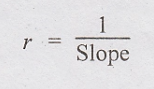
33.
Define dynamic resistance.
The
dynamic or ac resistance is the reciprocal of the slope V-I characteristics of
diode.
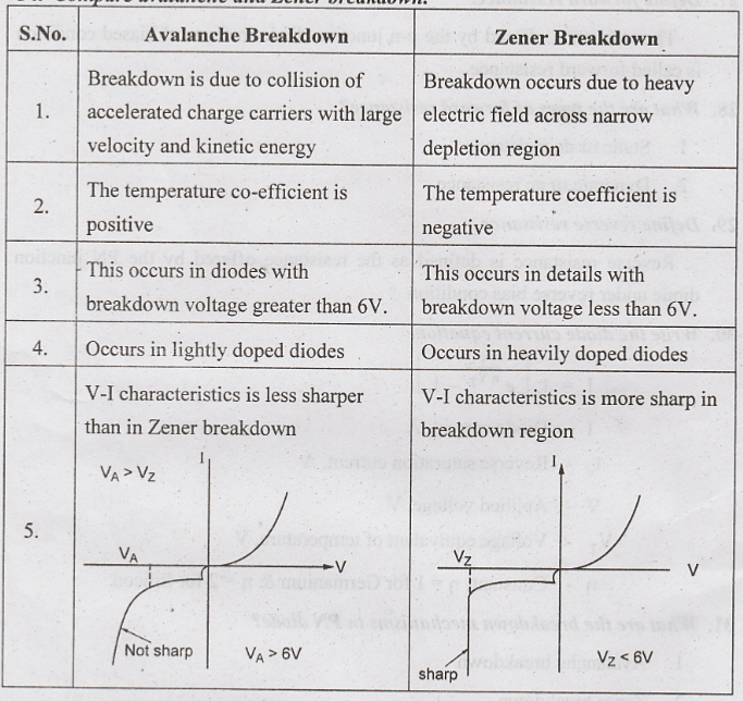
34.
Compare avalanche and Zener breakdown.
35.
Define diffusion capacitances.
It
is defined as the rate of change of injected charge with applied voltage.
36.
What are the applications of PN diode?
i.
Rectifier
ii.
Switch
iii.
Clippers
iv.
Clampers
v.
Detector
37.
Define Zener effect.
Due
to heavy doping, the electric field at the junction will be very high even at
low reverse voltage. The electrons in covalent bonds break away from the bonds.
This is called as Zener effect.
38.
What is Zener diode?
A
diode which exhibits Zener effect is called Zener diode.
39.
What are the applications of Zener diode?
i.
Voltage regulators
ii.
Zener limiters
iii.
Over-voltage protectors
40.
Define rectifier.
A
rectifier is an electrical device that converts alternating current (ac) to
direct current (dc).
41.
What are the types of rectifier?
i.
Half-wave rectifier
ii.
Full-wave rectifier
42.
What is half-wave rectifier?
It
converts an ac voltage into a dc voltage during one half of the ac cycle only.
43.
What is full wave rectifier?
It
converts an ac voltage into pulsating dc voltage during both half cycles of the
applied voltage.
44.
Define Ripple factor.
The
ratio of rms value of ac component to the dc component in the output is known
as ripple factor.
45.
Define efficiency.
Efficiency
is defined as the ratio of dc output power to ac input power.
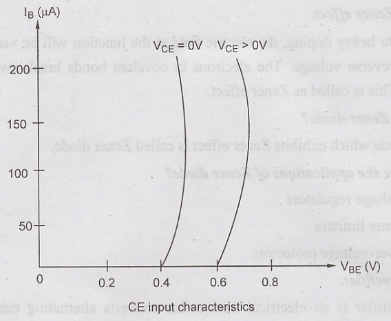
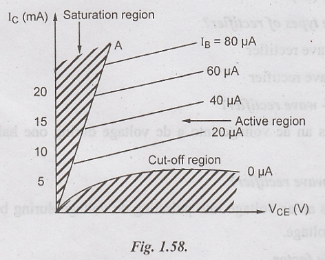
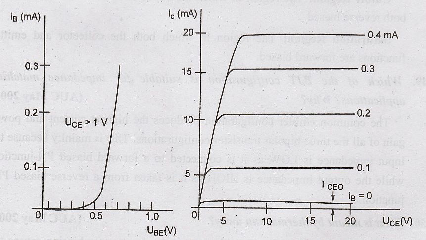
46. Draw the input and output characteristics of a transistor in CE configuration and mark the cutoff, saturation and active regions. (AUC May 2009)
47.
State the advantage of Optocoupler. (AUC May 2009)
i.
An optocoupler (or an optoelectronic coupler) is basically an interface between
two circuits which operate at different voltage levels. The key advantage of an
optiocoupler is the electrical isolation between the input and output circuits.
ii. They can replace relays and reed relays, giving much faster switching (2005 YEM speeds, no contact bounce, better reliability, and usually better electrical isolation except for special configurations. However relays have high current capability, higher output voltage, lower on resistance and offset voltage and higher off resistance.
iii.
They can replace pulse transformers in many floating applications. Opto-
isolators can transmit DC signal components and low frequency AC, whereas pulse
transformers couple only the high frequency components, (800 and a latch is
required to restore the DC information. Pulse transformers have faster rise
time than phototransistor optocouplers.
48.
Name the operating modes of a transistor. (AUC Nov 2010)
i.
Active region
ii.
Cut-off region
iii.
Saturation region
Active
Region: It is defined in which transistor function is biased in reverse
direction and emitter function in forward direction.
Cutoff
Region: The region in which the collector and emitter functions are both
reverse biased.
Saturation
Region: The region in which both the collector and emitter functions are
forward biased.
49.
Which of the BJT configuration is suitable for impedance matching applications?
Why? (AUC May 2007)
The
common emitter configuration produces the highest current and power gain of all
the three bipolar transistor configurations. This is mainl;y because the input
impedance is LOW as it is connected to a forward biased PN-junction, while the
output impedance is HIGH as it is taken from a reverse biased PN- junction.
50.
What is meant by thermal run away? (AUC May 2007)
The
continuous increase in collector current due to poor-biasing causes the (110
temperature at collector terminal to increase. If no stabilization i.e., done,
the collector leakage current also increases. This further increases the
temperature. This action becomes cumulative and ultimately the transistor turns
out. The self- destruction of an unstabilized transistor is known as thermal
runaway.
51.
Why is necessary to stabilize the operating point of transistor? (AUC Nov 2005)
In
order to keep the transistor operation in Active region, it is necessary to
stabilize the transistor. If not, the transistor may go out of active region.
(Saturation or cutoff region).
52.
Derive the relationship between a and B. (AUC Dec 2008)

53.
Draw and explain input and output characteristics of a transistor CB configuration.
(AUC May 2005)
54.
What is pinch off voltage? (AUC Dec 2011)
It
is the voltage at which the channel is pinched off, (i.e.,) all the free
charges ls from the channel get removed.
55. List the comparison between CB,CE,CC amplifiers. (AUC Dec 2007)
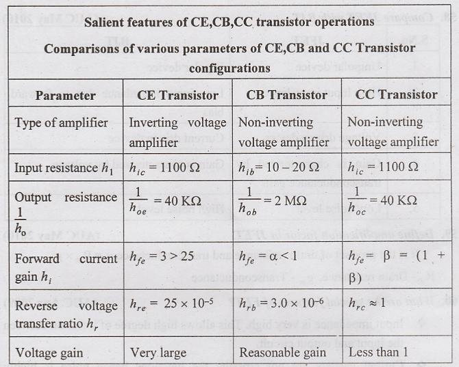
56.
State the biasing conditions required for the three regions of operations of a
BJT. (AUC May 2004)
Two
external voltage sources are used to establish the required bias conditions for
active-mode operation. The voltage VBE causes the p-type base to be
higher in potential than the n-type emitter, thus forward-biasing the emitter-
base junction. The collector-base voltage VCB causes the n-type
collector to be higher in potential than the p type base, thus reverse-biasing
the collector-base junction.
57.
Give any two differences between E-MOSFET and D-MOSFET. (AUC Dec 2011)
In
E-MOSFEThas no conducting channel between two terminal, source terminal and
gateterminal. Whereas in the D-MOSFET has conducting channel between these two
terminal, source and gate.
58.
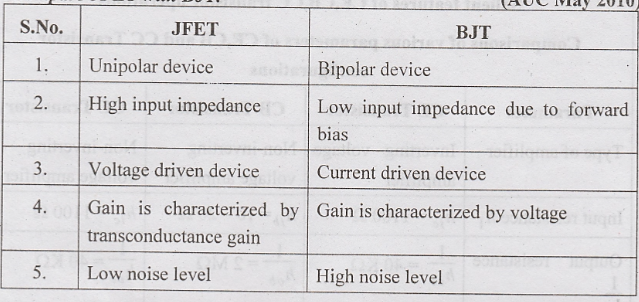
Compare JFET with BJT. (AUC May 2010)
59.
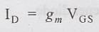
Define amplification factor in JFET. (AUC May 2010)
It
is the product of drain resistance and transconductance μ = Rd x gm
Rd
- Drain resistance, gm – Transconductance
60.
What are the special features of FET? (AUC Apr 2009)
i.
Input impedance is very high. This allows high degree of isolation between the
input and output circuit.
ii.
Current carriers are not crossing the junctions hence noise is highly reduced.
iii.
It has a negative temperature co-efficient of resistance. This avoids the
thermal runaway.
61.
Define: (a) Pinch off voltage and (b) Amplification factor in JFET. (AUC Apr
2009)
It
is the voltage at which the channel is pinched off, (i.e.,) all the free
charges from the channel get removed.
Amplification
factor is the product of drain resistance and trans conductance.
Μ
= Rd × gm
Rd
- Drain resistance, gm – Transconductance
62.
Why FET is called unipolar device? (AUC Dec 2004)
The
operation of FET depends upon the flow of majority carriers only either
hour
or electrons and hence FET is said to be unipolar device.
63.
Define Rd gm and μ of JFET. (May 2005)
The
change in the drain source voltage due to change in drain current with constant
VGS can be determined using the drain resistance rd
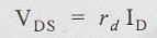
The
change in the drain current due to change in gate to source voltage can be
determined using the transconductance factor gm
64.
What do you understand by pinch off voltages and cutoff voltages? (AUC May
2006)
It
is the voltage at which the channel is pinched off, (i.e.,) all the free charges
from the channel get removed.
65.
List the important features of FET. (AUC Dec 2004)
i.
Input impedance is very high. This allows high degree of isolation between the
input and output circuit.
ii.
Current carriers are not crossing the junctions hence noise is highly reduced.
iii.
It has a negative temperature co-efficient of resistance. This avoids the
thermal runaway.
REVIEW QUESTIONS
1.
What is meant by donor impurity and acceptor impurity?
2.
Draw the energy band diagram for conductors, semiconductors and insulators.
3.
Explain in detail about extrinsic and intrinsic semiconductors.
4.
Explain the construction and operation of PN diode in forward and reverse bias
conditions.
5.
Draw the energy band diagram of a PN diode.
6.
Sketch the V-I characteristics of the PN diode.
7. What is diffusion capacitance of a semiconductor diode? Explain.
8.
Explain in detail about the current components in a PN diode.
9.
Explain about transition and depletion capacitance in detail and derive its
expression.
10.
Explain the breakdown mechanisms of a diode.
11.
What are the applications of a diode?
12.
Explain the construction and working of Zener diode.
13.
How does a Zener diode operate as voltage regulator? Explain.
14.
What do you mean by rectifier? How it is classified.
15.
Explain the static and dynamic resistance of a diode under forward and reverse
bias.
16.
Discuss briefly the temperature dependence characteristics of a PN diode.
17.
How PN diode acts as rectifier? Explain.
18.
Explain half wave rectifier in detail and derive its efficiency.
19.
Discuss in detail the operation of full wave rectifier and derive its
efficiency.
20.
Compare Half wave, Full wave and Bridge rectifiers.
21.
What is Zener effect? Explain the V-I characteristics of Zener diode.
22.
Derive the PN diode current equation.
23.
Draw the circuit for determining the transistor common base characteristics and
explain how the characteristics are measured and draw the graphs. (AUC DEC'11)
24.
Explain the switching characteristics of transistor with neat sketch. (AUC
NOV'10)
25. Describe the static input and output characteristics of a CB transistor with neat circuit diagram. (AUC NOV'10)
26.
Draw and explain the input and Output characteristics of a BJT in CE
configuration. (AUC APRIL'09)
27. (i) What are the factors against which an amplifier needs to be stabilized? (ii) Explain any one method of biasing a single stage BJT amplifier. (AUC MAY'04)
28.
Explain the construction and working of enhanced MOSFET and depletion MOSFET.
Draw the characteristics. (AUC DEC'11)
29. Explain how the transconductance of a JFET varies with drain current and gate voltage characteristics and transfer characteristics. (AUC MAY'10)
30.
A JFET has the following parameters IDDS = 32 mA, VGS(off)
= -8 Volts, VGS = -4.5 Volts. Find the values of drain current. (AUC
MAY'10)
31. (i) Explain the working of n-channel enhancement type MOSFET. Sketch its typical characteristics. (AUC MAY'09)
(ii)
Explain the application of FET as a voltage variable resistor. (AUC MAY'09)
Electronic Devices and Circuits: Unit I: Semiconductor Devices : Tag: : - Important Two Marks Questions with Answers on Semiconductor Devices
Related Topics
Related Subjects

Electronic Devices and Circuits
EC3353 - EDC - 3rd Semester - ECE Dept - 2021 Regulation | 3rd Semester ECE Dept 2021 Regulation