Electronic Devices and Circuits: Unit V: Power Amplifiers and DC/DC Converters
Important Solved Problems of Power Amplifiers and DC/DC Converters
Anna University Solved Problems
Anna University Important Solved Problems of Power Amplifiers and DC/DC Converters
SOLVED PROBLEMS
Problem 5.1
Design
a class B power amplifier to deliver an average power of 20 W to an 8 Ω load. VCC
is selected to be 5V greater than the peak output voltage. Determine the supply
voltage required, peak current drawn from each supply, total supply power,
power conversion efficiency. Also determine the maximum power that each
transistor must be able to dissipate safely.
Given:
PL
= 20 W
RL
= 8 Ω
Solution:

VCC
should be selected 5V greater than peak output voltage, Vo.
So,
VCC = 18 + 5 = 23 V
Peak
current drawn from each supply

Power
conversion efficiency, η = 
Maximum
power dissipation in each transistor

Problem 5.2
In
class AB amplifier, VCC = 15 V, RL = 100 Ω, and the
output is sinusoidal with a maximum amplitude of 10V. IS = 10-13A,
β = 50. Assume biasing diodes have one-third the junction area of the output
devices. Find the value of IBias that guarantees a minimum of 1 mA
through the diodes at all times. Determine the quiescent current and quiescent
power dissipation in the output transistors (Vo = 0). Also find VBB
for Vo = 0, +10V and -10V.
Given:
VCC
= 15 V
RL
= 100Ω
Vmax
= 10 V
IS
= 10-13 A
β
= 50
Solution:
Maximum
current iLmax = Vmax/R = 10/100 = 0.1 A = 100 mA
To
maintain a minimum current of 1 mA, IBias is selected as IBias
= 3 mA
It
is given that Biasing diodes have 1/3 junction area of output devices.
So,
quiescent current is 9 mA.
Quiscent power dissipation, P = 2 x 15 x 9 = 270 mW
For
Vo = 0,
Base
current IB through QN = 9/51 = 0.18 mA
So,
current flowing through diodes is 3 - 0.18 = 2.82 mA

At
Vo = + 10 V,
Current
through diodes will decrease to 1 mA.
Substitute
in VBB equation,
VBB
≈ 1.21 V
For
Vo = -10 V,
QN
will be conducting a very small current, so IB will be negligibly
small. Hence IBias of 3mA flow through the diodes.
Substitute
IB in VBB equation
VBB
≈ 1.26 V
Problem 5.3
A
BJT is specified to have a maximum power dissipation of 2 W at ambient
temperature of 25°C and a maximum junction temperature of 150°C. Find
(a)
Thermal resistance θ
(b)
Maximum power that can be safely dissipated at an ambient temperature of 50°C
(c)
Junction temperature if the device is operating at TA = 25°C and
dissipating 1W.
Given:
Maximum
power dissipation = 2 W
Ambient
Temperature TA = 25°C,
Maximum junction temperature = 150°C
Solution:

Problem 5.4
In
Figure R1 = 10 K Ω, R2 = 2.2 KΩ, RC = 3.6 KΩ,
RE = 1.1 KΩ VCC = +10V. Find the dc power drawn from the
supply by the amplifier.

Solution:

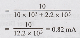
DC
voltage across R2 is

DC
voltage across R2,

DC
emitter current, IE = VE/RE

Total
DC current drawn from the supply is
IT
= IC + I1 = 1mA + 0.82 mA = 1.8 mA
DC
Power drawn from the supply is

Problem 5.5
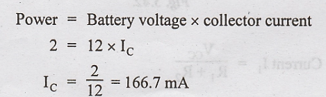
A
power amplifier operated from 12 V battery gives an output of 2W. Find the
maximum collector current in the circuit.
Solution:
Problem 5.6
In
CE amplifier shown in Figure, Assume βdc = βac = 100.
1.
Determine dc Q-point
2.
Determine voltage gain and power gain
3.
Signal power in load RL
4.
Efficiency

Solution:


Problem 5.7
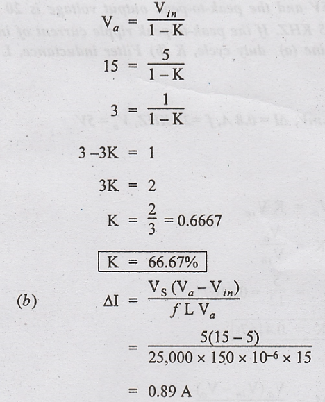
A
boost regulator has an input voltage of Vin = 5 V. The average
output voltage, Va = 15 V and the average load current, Ia
= 0.5 A. The switching frequency is 25 KHZ. If L = 150 μH and C = 220 μF.
Determine (a) duty cycle, k (b) ripple current of inductor, ∆I (c)Peak current
of inductor, I2, (d) ripple voltage of filter capacitor, VC
Given:
Vin = 5V, Va = 15 V, f = 25 KHZ, L=150 μH. C = 220 μF
Solution:
(a)
Duty Cycle

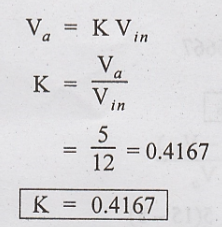
Problem 5.8
The
buck regulator has an input voltage of Vin = 12 V. The required
average output voltage is Va = 5V and the peak-to-peak output
voltage is 20 mV. The switching frequency is 25 KHZ. If the peak-to-peak ripple
current of inductor is limited to 0.8 A. Determine (a) duty cycle, K (b) Filter
inductance, L (c) filter capacitor C.
Given:
Vin
≈ 12 V, ∆VC = 20 mV, ∆I = 0.8 A, f = 25 KHZ, Va = 5V
Solution:
(a) Duty Cycle
(b) Filter Inductance, L

(c) Filter Capacitor, C

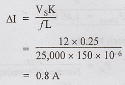
Problem 5.9
A
buck-boost regulator has an input voltage of Vin = 12 V. The
switching frequency is 25 KHZ. If L = 150 μH, C = 220μF. Duty cycle K = 0.25.
The average load current Ia = 1.25 A. Determine (a) average output
voltage, (b)Peak-to-peak output voltage ripple ∆VC (c) Peak-to-peak
ripple current of inductor ∆I, (d) peak current of the transistor IP.
Given
Vin
= 12 V, K = 0.25, Ia = 1.25 A, f = 25 KHZ, L = 150 μH, C = 220 μF
Solution:
(a) Average Output Voltage
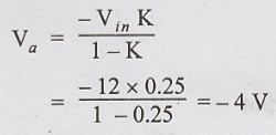
(b) Peak-to-Peak Output Voltage
Ripple

(c) Peak-to-Peak Ripple Current of
Inductor, ∆I
(d)Peak-peak current of the
transistor IP

Peak-peak
current of transistor

Problem 5.10
An
ideal class B complementary symmetry push pull amplifier operates with VCC
= 12 V and RL = 5 Ω, if the input is sinusoidal. Calculate (a)
maximum power output (b) Maximum power dissipation (c) power dissipation in
each transistor (d) conversion efficiency.
Given:
VCC
= 12 V
RL
= 5 Ω
Solution:
(b) Maximum Power Output

(b) Maximum Power Dissipation

(c) Power Dissipation in each
Transistor

(d) Efficiency
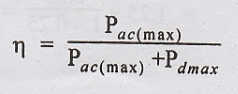

Problem 5.11
The
maximum collector dissipation of a transistor used in class A amplifier is 10
W. The collector efficiency of the circuit is 32%. Calculate the ac power
output.
Given:
η
= 32% = 32/100 = 0.32
Pd.c
= 10 W
To Find:
ac
power output, Po(ac)
Solution:

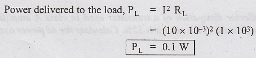
Problem 5.12
A
single transistor is operating as an ideal class B amplifier with 1 KΩ load. A
dc meter in the collector circuit reads 10 mA. How much power is delivered to
the load?
Given:
RL = 1ΚΩ= 1 x 10³ Ω
IC
= 10 mA = 10 x 10-3 A
To Find:
Power
delivered to the load
Solution:
Power delivered to the load,
Electronic Devices and Circuits: Unit V: Power Amplifiers and DC/DC Converters : Tag: : Anna University Solved Problems - Important Solved Problems of Power Amplifiers and DC/DC Converters
Related Topics
Related Subjects

Electronic Devices and Circuits
EC3353 - EDC - 3rd Semester - ECE Dept - 2021 Regulation | 3rd Semester ECE Dept 2021 Regulation