Electronic Devices and Circuits: Unit I: Semiconductor Devices
Forward Biased PN Junction
Reverse Biased P-N Junction, PN Diode Symbol
In unbiased PN junction, there is no flow of current, when forward bias is applied to the PN junction, the applied forward voltage creates an electric field opposite to the potential barrier.
FORWARD
BIASED PN JUNCTION
In
unbiased PN junction, there is no flow of current, when forward bias is applied
to the PN junction, the applied forward voltage creates an electric field
opposite to the potential barrier.
i.
Thus the potential barrier is reduced at the junction. As the potential barrier
is very small (0.7 V for Si and 0.3 V for Ge), a small forward voltage is
sufficient to eliminate the barrier potential.
ii.
The applied positive potential repels the holes in P-type region towards the
junction. The electrons in the n-type region are also repelled towards the junction
due to the negative voltage applied in n-region.

iii.
When the applied potential is more than the internal barrier potential, the
depletion region completely disappears and the junction resistance becomes
zero.
iv.
The junction provides a low resistance path and thus current flows in the
circuit. This current is called forward current.
v.
When the forward voltage is increased, the large number of majority charge
carriers can cross the junction. These large number of majority charge carriers
constitute the forward current.
The
current in P - region is due to the movement of holes which are majority
carriers. This is called hole current.
The
current in the n-regions is due to the movement of free electrons which are
majority carriers. This is called electron current. The overall forward current
is due to the majority charge carriers.
These
majority carriers can travel around the closed circuit and large amount of
current flows from negative to positive of the battery.
The
direction of conventional current is from positive to negative of the battery
which is opposite to the direction of flow of electrons.
The
voltage drop across a p- n junction diode in forward biased condition is made
up of
(i)
drop due to barrier potential
(ii)
drop due to internal resistance
REVERSE BIASED P-N JUNCTION
The
P-region is connected to negative terminal of the battery and n -region is
connected to positive terminal of the battery.
When
p-n junction is reverse biased, the negative terminal attracts the holes in p -
region and the positive terminal attracts the free electrons in n - region away
from the junction.
The
electrons and holes move away from the junction and the width of depletion
region increases.
The charge carriers are unable to cross the junction.
Thus
there are more positive ions in the n- region and more negative ions in the p-
region.
When
the depletion region widens, the barrier potential across the junction also
increases.
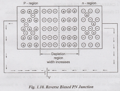
The
applied reverse voltage creates an electric field which is in same direction of
potential barrier and thus the barrier width is increased.
This
increased potential barrier prevents the flow of charge carriers across the
junction.
When
PN junction is reverse biased, it has high resistance path and no current flows
in the circuit.
After certain extent, the junction breakdown occurs. Then a small amount of current flows through it due to minority charge carriers i.e., the electrons on p-side and holes on n- -side constitute current in reverse biased condition. So, the reverse current is always very small. The reverse current remains constant even if the reverse voltage is increased upto a certain limit. Hence, it is called Reverse saturation current. The magnitude of reverse saturation current depends on junction temperature.
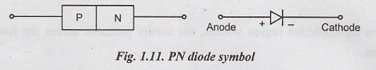
PN DIODE
SYMBOL
V-I
CHARACTERISTICS OF PN DIODE
Fig.1.12
shows the circuit for V-I characteristics of PN junction diode.
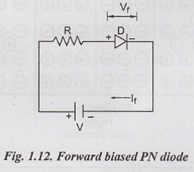
V-I
characteristics is used for studying the response of p - n junction.
It
is defined as the graph of voltage applied across the p-n junction and the
current flowing through the p-n junction.
As
shown in Fig.1.13, the applied voltage is V and the voltage across the diode is
Vf.
The
current flowing in the circuit is the forward current If. The graph
of forward current If, against the forward voltage Vf
across the diode is called forward characteristics of a diode.
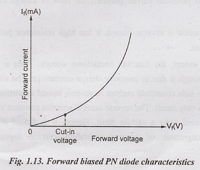
As
voltage is applied, the current flow is very small upto the cut-in voltage VC
or threshold voltage VTh. or knee voltage.
When
the applied voltage exceeds the threshold voltage the width of the depletion
region is further reduced and the forward current rises exponentially as shown
in Fig.1.13. If the forward voltage is increased beyond a certain value,
extremely large amount of current is produced which may destroy the diode due
to overheating.
The
point after which the current starts increasing exponentially is called Knee of
the curve.
Reverse Bias
The
Fig. 1.14 shows the reverse biased p- n diode. The reverse voltage across the
diode is VR and the current flowing through the diode is reverse
current IR. The reverse current is mainly due to minority charge
carriers. The graph of reverse current IR versus reverse voltage VR
is called reverse characteristics of a diode.

During
reverse bias, all the majority carriers are attracted by the battery i.e.,
holes from P-type move towards negative terminal of battery and electrons from
n-type move towards positive terminal of battery. Thus only immobile ions near
the junction form a strong depletion region which offers very high resistance
for majority carriers.
Hence only very small current flows in the circuit. The polarity of reverse voltage applied is opposite to that of forward voltage. So, the reverse saturation current is opposite to the forward current and its value is negative.
i.
When reverse voltage is increased, reverse current increases initially upto
certain voltage. After some extent, the current remains constant although
reverse voltage is increased. This current is called reverse saturation current
Io the point at which breakdown occurs and reverse saturation
current increases rapidly is called knee of the reverse characteristics.

Electronic Devices and Circuits: Unit I: Semiconductor Devices : Tag: : Reverse Biased P-N Junction, PN Diode Symbol - Forward Biased PN Junction
Related Topics
Related Subjects

Electronic Devices and Circuits
EC3353 - EDC - 3rd Semester - ECE Dept - 2021 Regulation | 3rd Semester ECE Dept 2021 Regulation