Electronic Devices and Circuits: Unit I: Semiconductor Devices
Field Effect Transistor (FET)
Types, Junction Field Effect Transistor (JFET) | Semiconductor Devices
The FET is a device in which the flow of current through the conducting region is controlled by an electric field, hence the name Field Effect Transistor (FET). As current conduction is only by majority carriers, FET is said to be a unipolar device.
FIELD EFFECT TRANSISTOR
The
FET is a device in which the flow of current through the conducting region is
controlled by an electric field, hence the name Field Effect Transistor (FET).
As current conduction is only by majority carriers, FET is said to be a
unipolar device.
Based on the construction, the FET can be classified into two types - Junction Field Effect Transistor (JFET) and Metal Oxide Semiconductor Field Effect Transistor (MOSFET).
JUNCTION FIELD EFFECT TRANSISTOR (JFET)
JFET
is classified into two types, namely
(i)
N-channel JFET with electrons as the majority carriers and
(ii)
P-channel JFET with holes as the majority carriers.
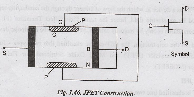
CONSTRUCTION OF
N-CHANNEL JFET
It
consists of a N-type bar which is made of silicon ohmic contacts (terminals)
made at the two ends of the bar, are called source and drain.
Source
(S)
This
terminal is connected to the negative pole of the battery. Electrons which are
the majority carriers in the N-type bar enter the bar through this terminal.
Drain
(D)
This
terminal is connected to the positive pole of the battery. The majority
carriers leave the bar through this terminal.
Gate
(G)
Heavily doped P-type silicon is diffused on both sides of the N-type silicon bar by which PN junctions are formed. These layers are joined together and called Gate G.
Channel
The
region BC of the N-type bar between the depletion region is called the channel.
Majority carriers move from the source to drain when a potential difference VDS
is applied between the source and drain.
OPERATION OF
N-CHANNEL JFET
When
VGS = 0 and VDS = 0 when no voltage is applied between
drain and source, and gate and source, the thickness of the depletion regions
round the PN junction is uniform as shown in Fig. 1.46.
Case
(i)
When
VDS = 0 and VGS is decreased from zero. In this case, the
PN junctions are reverse biased and hence the thickness of the depletion region
increase. As VGS is decreased from zero, the reverse bias voltage
across the PN junction is increased and hence, the thickness of the depletion
region in the channel until the two depletion regions make contact with each
other. In this condition, the channel is said to be cut-off. The value of VGS
which is required to cut-off the channel is called the cut-off voltage VC.
Case
(ii)
When VGS = 0 and VDS increased from drain is positive with respect to the source with VGS = 0.
Now
the majority carriers (electrons) flow through the N-channel from source to
drain. Therefore the conventional current ID flows from drain to source.
The magnitude of the current will depend on the following factors.
i.
The number of majority carriers (electrons) available in the channel. i.e., the
conductivity of the channel.
ii.
The length L of the channel.
iii.
The cross-sectional area A of the channel at B.
iv.
The magnitude of the applied voltage VDS. Thus the channel acts as a
resistor of resistance R is given by
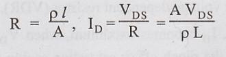
Where
ρ is the resistivity of the channel. Because of the resistance of the channel
and the applied voltage VDS, there is a gradual increase of positive
potential along the channel from source to drain. Thus the reverse voltage
across the PN junctions increases and hence the thickness of the depletion
regions also increases. Therefore, the channel is wedge shaped as shown in Fig.
1.47.
As VDS is increased, the cross-sectional area of the channel will be reduced. At a certain value VP of VDS, the cross-sectional area at B becomes minimum. At this voltage, the channel is said to be pinched off and the drain voltage VP is called the pinch-off voltage.
As
a result of the decreasing cross-section of the channel with increase of VDs,
the following results are obtained.
i.
As VDS is increased from zero, ID increases along OP, and
the rate of increase of ID with VDS decreases as shown in
Fig. 1.48. The region from VDS = 0 V to VDS = VP
is called the ohmic region. In the channel ohmic region the drain to source
resistance VDS/ID is related to the gate voltage VGS
in an almost linear manner. This is useful as a voltage variable resistor (VVR)
or voltage dependent resistor (VDR).
ii.
When VDS = VP, ID becomes maximum, when VDS
is increased beyond VP, the length of the pinch-off or saturation
region increases. Hence there is no further increase of ID.

iii. At a certain voltage corresponding to the point B, ID suddenly increases. This effect is due to the Avalanche multiplication of electrons caused by breaking of covalent bonds of Silicon atoms in the depletion region between the gate and the drain. The drain voltage at which the breakdown occurs is denoted by B VDGO. The variation of ID with VDS when VGS = 0 is shown in Fig. 1.48, by the curve OPBC.
Case (iii)
When
VGS is negative and VDS is increased.
When
the gate is maintained at a negative voltage less than the negative cut-off
voltage, the reverse voltage across the junction is further increased. Hence
for a negative value of VGS the curve of ID versus VDS
is similar to that for VGS = 0, but the values of VP and
B VDGO are lower as shown in Fig. 1.48.
From
the curves, it is seen that above the pinch-off voltage, at a constant value of
VDS, ID increases with an increase of VGS.
Hence a JFET is suitable for use as a voltage amplifier, similar to a
transistor amplifier.
It
can be seen from the curve that for voltage VDS = VP, the
drain current is not reduced to zero. If the drain current is reduced to be
zero, the ohmic voltage drop along the channel should also be reduced to zero.
Further the reverse biasing to the gate source PN junction essential for
pinching off the channel would also be absent.
The
drain current ID is controlled by the electric field that extends
into the channel due to reverse biased voltage applied to the gate hence, this
device has been given the name Field Effect Transistor.
In a bar of P type semiconductor, the gate is formed due to N-type semiconductor. The working of the P-channel JFET will be similar to that of N channel JFET with proper alterations in the biasing circuits, in this case holes will be the current carriers instead of electrons.
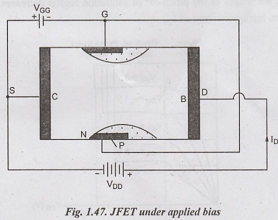
The
circuit symbols for N-channel and P-channel JFETs are shown in Fig.1.49. It
should be noted that the direction of the arrow points in the direction of
conventional current which would flow into gate if the PN junction was forward
biased.
CHARACTERISTICS
PARAMETERS OF THE JFET
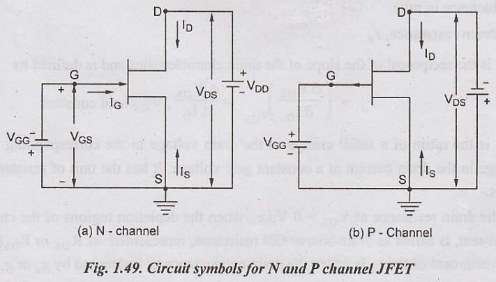
In
a JFET, the drain current ID depends upon the drain voltage VDS
and the gate voltage VGS. Any one of these variables may be fixed
and the relation between the other two are determined. These relations are
determined by the three parameters which are defined below.
i.
Mutual Conductance (or) Transconductance, gm
It
is the slope of the transfer characteristic curves, and is defined by
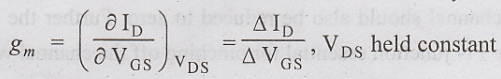
It
is the ratio of a small change in the drain current to the corresponding small
change in the gate voltage at a constant drain voltage. The change in ID
and VGS should be taken on the straight part of the transfer
characteristics. It has the unit of conductance in mho.
ii. Drain resistance, rd
It
is the reciprocal of the slope of the drain characteristics and is defined by
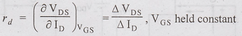
It
is the ratio of a small change in the drain voltage to the corresponding small
change in the drain current at a constant gate voltage. It has the unit of
resistance in ohms.
The
drain resistance at VGS = 0 V, i.e., when the depletion regions of
the channel are absent, is called as drain-source ON resistance, represented as
RDS or RDS (ON). The reciprocal of the rd is
called the drain conductance. It is denoted by gd or gos.
iii.
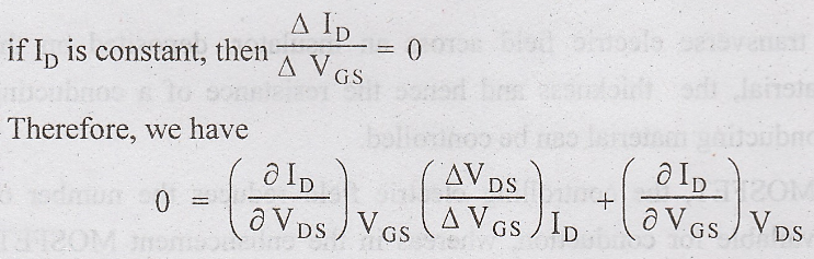
Amplification Factor, μ
It
is denoted by
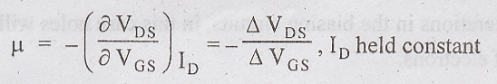
It
is the ratio of a small change in the drain voltage to the corresponding small
change in the gate voltage at a constant drain current. Here the negative sign
shows that when VGS is increased, VDS must be decreased
for ID to remain constant.
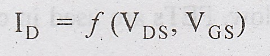
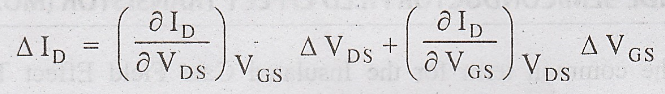
(iv) Relationship Among
FET parameters
As
ID depends on VDS and VGS the functional
equation can be expressed as
If
the drain voltage is changed by a small amount from VDS to (VDS
+ ∆ VDS) and the gate voltage is changed by a small amount from VGS
to (VGS + ∆ VGS). Then the corresponding small change in
ID may be obtained by applying Taylor's theorem with neglecting
higher order terms. Thus the small change ∆ ID is given by
Dividing
both the sides of this equation by ∆ VGS, we obtain
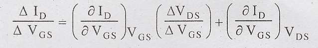
substituting
the values of the partial differential coefficients, we get
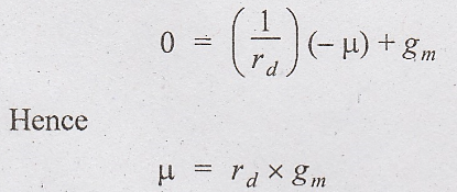
Therefore,
amplification factor (µ) is the product of drain resistance (rd) and
transconductance (gm).
(v)
Power Dissipation, PD
The FET's continuous power dissipation PD is the product of ID and VDS·
Application of FET
1.
FET is used as a buffer in measuring instruments receivers since it has high
input impedance and low output impedance.
2.
FETs are used in RF amplifiers in FM tuners and communication equipment for the
low noise level.
3.
Since the input capacitance is low, FETs are used in cascade amplifiers in
measuring and list equipments.
4.
Since the device is voltage controlled, it is used as a voltage variable
resistor in operational amplifiers and tone controls.
Electronic Devices and Circuits: Unit I: Semiconductor Devices : Tag: : Types, Junction Field Effect Transistor (JFET) | Semiconductor Devices - Field Effect Transistor (FET)
Related Topics
Related Subjects

Electronic Devices and Circuits
EC3353 - EDC - 3rd Semester - ECE Dept - 2021 Regulation | 3rd Semester ECE Dept 2021 Regulation