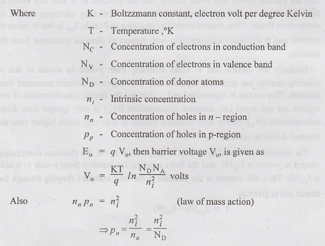
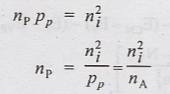
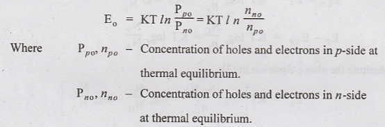
Electronic Devices and Circuits: Unit I: Semiconductor Devices
Energy Band Structure of Open Circuited PN Junction
Derivation
Consider the unbiased PN junction and to know the energy band structure, we have to analyze the Fermi level of the semiconductor material.
ENERGY BAND STRUCTURE OF OPEN CIRCUITED PN JUNCTION
Consider
the unbiased PN junction and to know the energy band structure, we have to
analyze the Fermi level of the semiconductor material. Fermilevel is defined as
the particular energy level where the probability of occupation is 50%. For an
n- type semiconductor, there are more electrons in the conduction band than
there are holes in the valence band. This implies that the probability of
finding an electron near the conduction band is larger than that of finding a
hole at the valence band. So, the Fermilevel is closer to the conduction band
in an n-type semiconductor.
For p-type semiconductor, there are more holes in the valence band than the electrons in the conduction band. Thus probability of finding an electron near the conduction band is smaller than the probability of finding a hole at the valence band. Therefore, the Fermilevel is closer to the valence band in a P-type semiconductor.
When
a PN junction is formed, the energy levels of these regions will undergo a
relative shift to make the Fermilevel constant throughout the diode. This
equalization is similar to equalization of levels of water in two containers
i.e., when two semiconductor materials are joined, the flow of charge carriers
occur until the fermilevels in the two materials are equalized. We know that
Fermilevel EF is closer to the conduction band ECN in n
type semiconductor and it is closer to the valence band EVP in
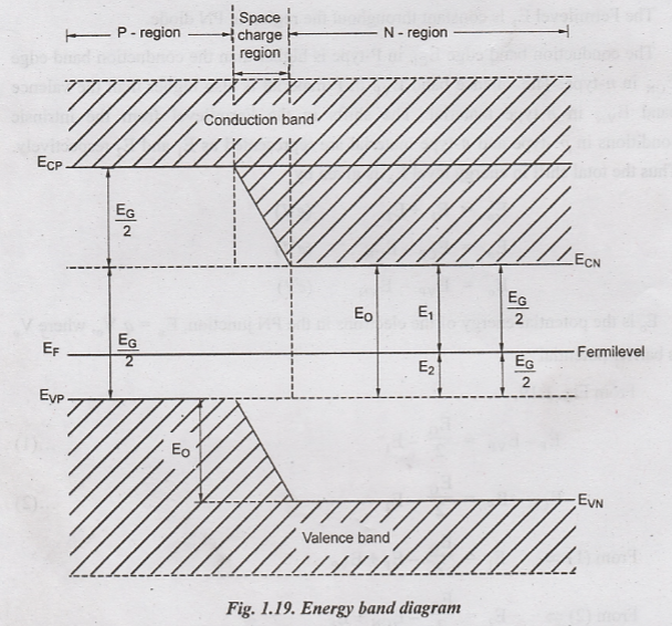
P-type semiconductor as shown in Fig. 1.19.
The
Fermilevel EF is constant throughout the region in PN diode.
The
conduction band edge ECP in P-type is higher than the conduction
band edge ECN in n-type. The valence band EVP in P material is also
higher than the valence band EVN in n-type material. The shifts in
the Fermilevel from the intrinsic conditions in p -type and n-type material are
represented as E1 and E2 respectively. Thus the total
shift in energy level Eo is given by
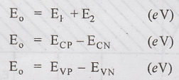
Eo
is the potential energy of the electrons in the PN junction, Eo = q
Vo, where Vo is barrier potential
From
Fig. 1.19,
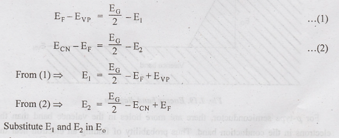
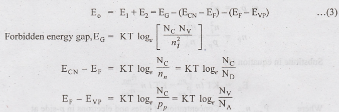
Substitute the above equation in (3)
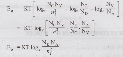
Substitute
in equation (4)
Electronic Devices and Circuits: Unit I: Semiconductor Devices : Tag: : Derivation - Energy Band Structure of Open Circuited PN Junction
Related Topics
Related Subjects

Electronic Devices and Circuits
EC3353 - EDC - 3rd Semester - ECE Dept - 2021 Regulation | 3rd Semester ECE Dept 2021 Regulation