Electronic Devices and Circuits: Unit III: Multistage Amplifiers and Differential Amplifier
Dual Input, Unbalanced Output Differential Amplifier
Single Input Balanced Output Differential Amplifier, Single Input Unbalanced Output Differential Amplifier
The dual input unbalanced output differential amplifier. It has two inputs and the output voltage is measured only at one collector with respect to ground.
DUAL INPUT, UNBALANCED OUTPUT DIFFERENTIAL AMPLIFIER
The dual input unbalanced output differential amplifier is shown in Fig.3.20. It has two inputs and the output voltage is measured only at one collector with respect to ground.

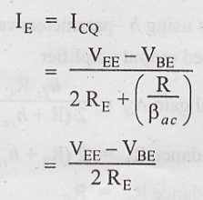
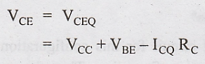
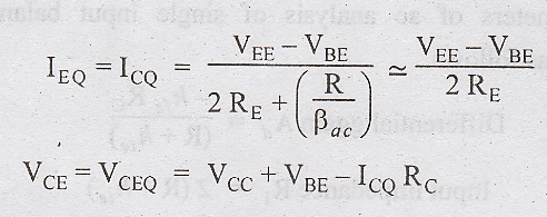
DC Analysis
As
the biasing of this circuit is identical to that of the dual input balanced
output- circuit, the output of the dc analysis will be identical.
Thus
the values of ICQ and VCEQ are obtained as

AC Analysis
The
result of ac analysis using h-parameters can be obtained in a similar method as
that for dual input balanced output amplifier.
Differential
gain 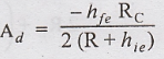
Input
impedance 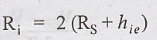
Output impedance RO = RC
The
differential gain is reduced to 50% compared to dual input balanced output
amplifier. The input and output impedances remain unchanged.
SINGLE INPUT, BALANCED OUTPUT DIFFERENTIAL AMPLIFIER

The
input signal is applied only to the base of Q1 transistor with the
other input connected to ground. The output is taken between the collector
terminals C1 and C2. Since both the collector terminals
are at the same dc potential, the output is called as "balanced
output". The single input balanced output differential amplifiers is shown
in Fig. 3.21.
DC Analysis
The
same procedure is followed for the dc analysis because the dc equivalent
circuit for all these configurations is the same.
AC Analysis
The
parameters of ac analysis of single input balanced output differential amplifier
are as follows.
Differential
gain 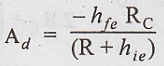
Input
impedance 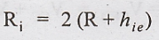
Output
impedance RO = RC
The
gain is same as that of dual input balanced output configuration.
SINGLE INPUT UNBALANCED OUTPUT DIFFERENTIAL AMPLIFIER
The
single input unbalanced output differential amplifier is shown in the Fig.3.22.
The input is applied to the base of Q1 transistor and the output is
measured at collector terminal C2 with respect to ground. This
configuration is rarely used in practice.

DC Analysis
The
dc equivalent circuit for this configuration is identical to that of the dual
input, balanced output configuration. Thus the expressions for ICQ
and VCEQ are obtained as
AC Analysis
The
result of analysis of single input unbalanced output differential amplifier is
obtained as follows

The
gain is same as that of dual input unbalanced output configuration.
Improving CMRR
CMRR
is the figure of merit of a differential amplifier. CMRR should be as high as
possible. We know that CMRR is the ratio of differential voltage gain Ad
and common mode voltage gain Ac. Thus CMRR can be increased by
i.
Increasing Ad
ii.
Decreasing Ac
Effect of Emitter Resistor RE
RE
will not introduce any negative feedback for differential mode operation. Hence
Ad does not depend on the value of RE. But RE introduces
a negative feedback in common mode operation, this inturn reduces the common
mode gain.
If RE increases, negative feedback is also increased and the common mode gain is reduced. Hence CMRR will increase.
If
RE value is changed, then Q point will be shifted. Thus we have to
go for other methods to improve CMRR, such as
i.
Constant current bias
ii.
Current mirror circuit
iii.
Active load.
Electronic Devices and Circuits: Unit III: Multistage Amplifiers and Differential Amplifier : Tag: : Single Input Balanced Output Differential Amplifier, Single Input Unbalanced Output Differential Amplifier - Dual Input, Unbalanced Output Differential Amplifier
Related Topics
Related Subjects

Electronic Devices and Circuits
EC3353 - EDC - 3rd Semester - ECE Dept - 2021 Regulation | 3rd Semester ECE Dept 2021 Regulation