Electronic Devices and Circuits: Unit V: Power Amplifiers and DC/DC Converters
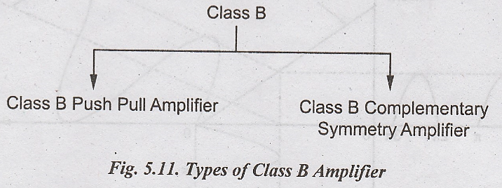
Class B Power Amplifiers
Class B Push Pull Amplifier
The main drawback of class A amplifier is that all of the supply power is dissipated in the transistor when there is no input.
CLASS-B POWER AMPLIFIER
The
main drawback of class A amplifier is that all of the supply power is
dissipated in the transistor when there is no input.
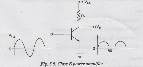
The
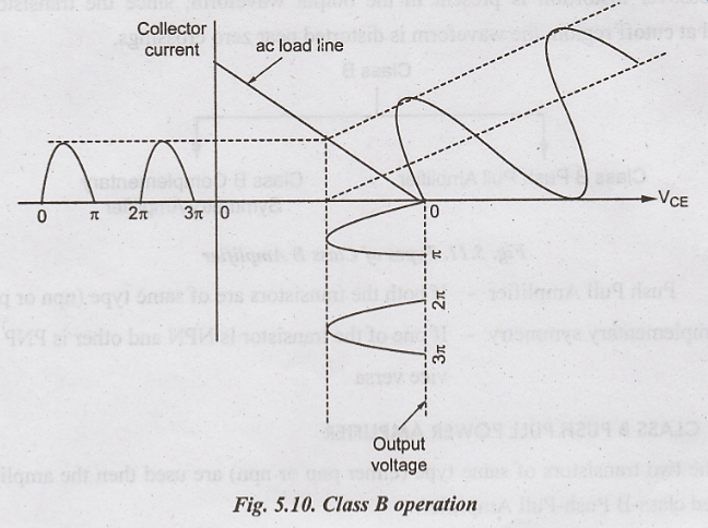
output power is obtained for one half cycle of input only. The collector
current flows for 180° only. The Q-point is adjusted to be in cutoff region i.e
IB = 0, VCE = VCC
The
transistor is in conduction state during positive half cycle of the signal and
in cutoff state during negative half cycle of the signal. Therefore, the output
signal is highly distorted.
Since
the transistor conducts for one half cycle of the input, the power dissipation
of these class B amplifiers are very less. Hence efficiency is increased.
Advantages
1.
Impedance with load is possible
2.
Second harmonic is cancelled automatically
3.
Zero power dissipation
4.
Higher efficiency than class A amplifiers
Disadvantages
Crossover
distortion is present in the output waveform, since the transistor is biased at
cutoff region, the waveform is distorted near zero crossings.
Push
Pull Amplifier - If both the transistors are of same type (npn or pnp)
Complementary
symmetry - If one of the transistor is NPN and other is PNP or vice versa
CLASS B PUSH PULL POWER AMPLIFIER
If the two transistors of same type (either pnp or npn) are used then the amplifier is called class-B Push-Pull Amplifier.
Construction
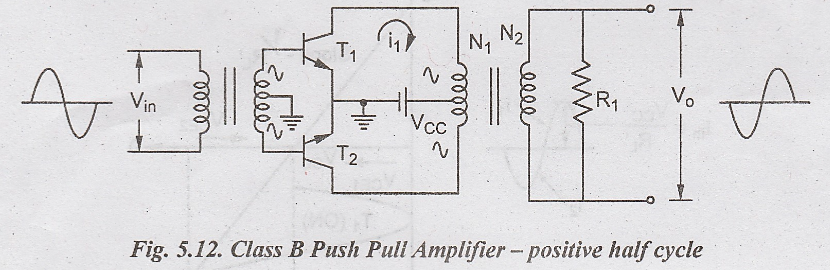
The
push-pull amplifier uses two centre tapped transformers. For getting full input
signal we use push pull circuit. In push-pull amplifiers, two transformers are
used, one at the input and the other at the load side. The transformer on the
input side is known as driver transformer and the transformer on the load side
is called as output transformer. Both are centre tapped transformers. Consider
the transformers coupled push pull amplifier shown in Fig.5.12.
Operation
When
Vin = 0, both transistors, T1 and T2 are cut
off. For positive half input cycle, T1 goes ON and current i, flows
in the direction as shown in Fig.5.12.
For
negative half cycle of input, T2 goes ON and a current i2
flows in the direction as shown in Fig.5.13.
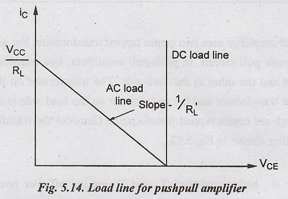
When
Vin= 0, VCC appears across both the transistors. Since de
resistance of transformer winding is negligible, dc loadline is almost
vertical.
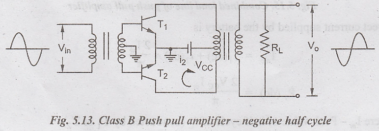
Fig. 5.14 shows load lines for class B pushpull amplifier.
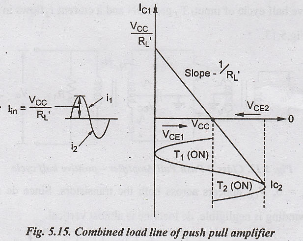
When
Vin is zero, resistance R'L is present in i1
to i2. Current i1 is taken as positive and i2
is in anticlockwise and is negative. The combination of these two half cycles
is shown in Fig.5.15.
Direct
current supplied by the battery is
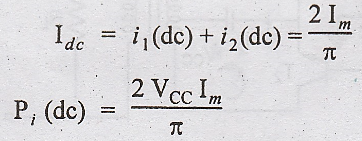
where
Im - Peak value of half cycle of iC (conducted by T1
or T2)
Electronic Devices and Circuits: Unit V: Power Amplifiers and DC/DC Converters : Tag: : Class B Push Pull Amplifier - Class B Power Amplifiers
Related Topics
Related Subjects

Electronic Devices and Circuits
EC3353 - EDC - 3rd Semester - ECE Dept - 2021 Regulation | 3rd Semester ECE Dept 2021 Regulation