Electronic Devices and Circuits: Unit V: Power Amplifiers and DC/DC Converters
Buck Regulator
Buck Converter, Operation, Derivations, Advantages, Disadvantages, Applications
Buck converter is also known as step down converter and produces a lower output voltage than input voltage. The average output voltage is less than the input voltage.
BUCK REGULATOR
Buck
converter is also known as step down converter and produces a lower output
voltage than input voltage. The average output voltage is less than the input
voltage. Fig.5.31 shows the circuit diagram of a buck regulator using power
BJT.

i.
The switch is implemented by using BJT, MOSFET or IGBT. The duty cycle varies
from 0 to 1.
ii.
The output voltage has harmonics which requires DC filter for smoothing out
ripples.
iii.
Gating signal is obtained by comparing the gating signal with de signal and
hard limiting the difference signal to obtain a square wave pulse.
iv.
The control circuit switches the transistor Q1 between ON and OFF
states. The indicator current forward biases the diode D1 and D1
conducts for the remaining switching period. This diode is known as Free
Wheeling Diode.
Operation
The
circuit operates in 2 modes.
Mode 1

At
t = 0, Q1 is switched ON.
i.
The input current flows through filter (L and C) inductor and capacitor and
load resistor. Fig.5.32 shows the equivalent circuit for Mode 1.
Mode 2
At
t = t1, Q1 is Switched OFF.
i.
The free wheeling diode D1 conducts due to energy stored in
inductor.
ii.
The inductor current flows through L, C, Load and diode D, until Q1
is switched ON in the next cycle.
Fig.5.33
shows the equivalent circuits for Mode 2.


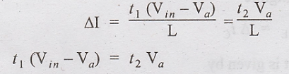
For
continuous current flow in the inductor L, The voltage and current waveform are
shown in Fig.5.34. The inductor current may be discontinuous depending on the
switching Frequency, filter inductance and Capacitance.
The
voltage across the inductor L is

Assume
that inductor current rises linearly from I1 to I2 in
time t1,


In
time t2, inductor current falls linearly from I2 to I1.

where
ΔI - peak to peak ripple current of inductor L Equate (3) and (6)
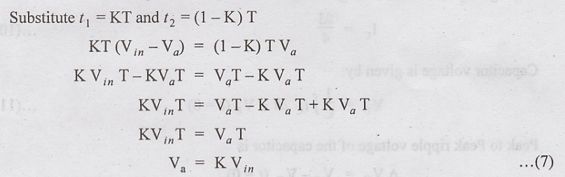
Assume
lossless transistor,

Average
input current,
IS
= K Ia
Switching
period T is given by
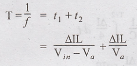

Using
KCL,
Load
current is written as
iL
= iC + io ...(9)
Δio
is very small and negligible
ΔiL
= ΔiC
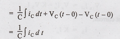
Average
capacitor current is given by
IC
= ΔI/4 ...(10)
Capacitor
voltage is given by

Peak
to Peak ripple voltage of the capacitor is
ΔVC
= VC - VC (t=0)
Substitute
(11)
Substitue
(10)


Substitute
(8) in (12)

The
converter produces a dc output voltage which is controllable through the duty
cycle D.
The
conversion ratio is defined as the ratio of the dc output voltage V0
to dc input voltage Vin under steady-state conditions.

For
bulk converter,
M(D)
= K
Advantages
1.
Requires only one transistor
2.
Simple construction
3.
High efficiency
4.
Less expensive
Disadvantages
1.
di/dt of the load current is limited by inductor
2. Smoothing input filter is required
3.
Need protection circuit to avoid short circuits
4.
Input current and charging current of output capacitor is discontinuous which
require large filter size.
Applications
1.
Used to drive high current loads, used in PCs, mother boards
2.
Battery chargers
3.
Solar chargers
Electronic Devices and Circuits: Unit V: Power Amplifiers and DC/DC Converters : Tag: : Buck Converter, Operation, Derivations, Advantages, Disadvantages, Applications - Buck Regulator
Related Topics
Related Subjects

Electronic Devices and Circuits
EC3353 - EDC - 3rd Semester - ECE Dept - 2021 Regulation | 3rd Semester ECE Dept 2021 Regulation