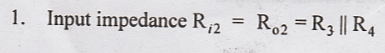
Electronic Devices and Circuits: Unit III: Multistage Amplifiers and Differential Amplifier
BISMOS Amplifier
FET Cascade Amplifier
The common gate amplifier stage is connected in cascade with a common source amplifier stage.
BIMOS AMPLIFIER
The
common gate amplifier stage is connected in cascade with a common source
amplifier stage.
Common Source (CS) Amplifier
i.
High Rin
ii.
Large transconductance
Common Gate (CG) Amplifier
i.
Current buffer
ii.
High frequency response
Fig.3.3 shows the BIMOS cascade amplifier. The Common Source (CS) transistor Q1 conducts a current signal due to input signal voltage Vi.
The
output in its drain terminal is fed to the source of Common Gate (CG)
transistor Q2. The output of Q2 is sent to its drain and
the load RL.
Q2
transistor acts as a buffer, offering low input impedance to Q1
drain and high impedance at output.
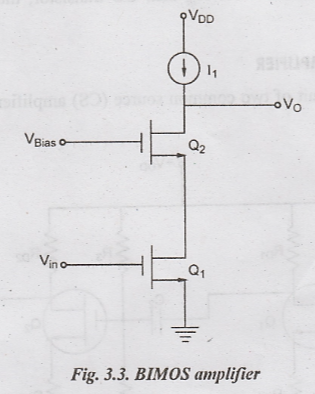
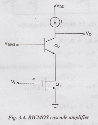
Fig.3.4
shows the combination of both BJT and FET in cascode operation.
MOSFET
provides an infinite input resistance, while BJT provides larger output resistance.
BJT
CB transistor provides lower Rin than CG transistor, thus reducing
Miller effect in Q1.
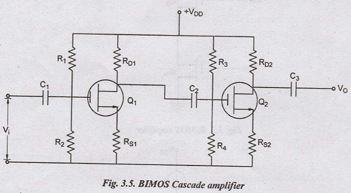
FET CASCADE AMPLIFIER
Fig.3.5
shows the circuit of two common source (CS) amplifier stages connected in
cascade.
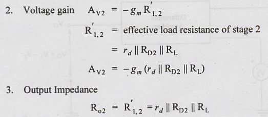
Stage 1:
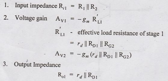
Stage 2:
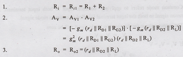
Cascaded Amplifier
The
overall parameters of the cascaded two stage amplifier are
Electronic Devices and Circuits: Unit III: Multistage Amplifiers and Differential Amplifier : Tag: : FET Cascade Amplifier - BISMOS Amplifier
Related Topics
Related Subjects

Electronic Devices and Circuits
EC3353 - EDC - 3rd Semester - ECE Dept - 2021 Regulation | 3rd Semester ECE Dept 2021 Regulation