Electronic Devices and Circuits: Unit III: Multistage Amplifiers and Differential Amplifier
Basic Differential Amplifier
Operation, Analysis, Summary
The input signals are given to both the input terminals and so it is called as "dual input". The output is taken between the collectors of the two transistors. Hence, it is called as "balanced output". As the output is the difference between the output of two collectors, it is called differential output. Thus, the amplifier is called dual input balanced output differential amplifier.
BASIC DIFFERENTIAL AMPLIFIER
The
two identical emitter biased circuits are used to form the differential
amplifier. The transistors Q1 and Q2 have identical
characteristics RE1 = RE2, RC1 = RC2
and VCC = |-VEE|.
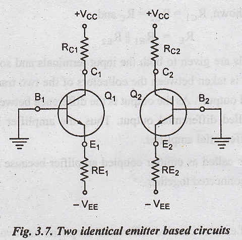
Fig. 3.7 shows two identical emitter biased circuits. These two emitter biased circuits are combined by connecting + VCC supply voltages of the two circuits together and -VEE Supply voltages together.
The
emitter E1 of transistor Q1 is connected to the emitter E2
of transistor Q2. Thus, RE1 is connected in parallel with
RE2.
The
input signal V1 is applied to the base B1 of transistor Q1
and V2 is applied to the base B2 of transistor Q2.
The output voltage is obtained between the collectors C1 and C2.

In
the Fig. 3.8 shown, RC1 = RC2 = RC and
RE
= RE1 || RE2
The
input signals are given to both the input terminals and so it is called as
"dual input". The output is taken between the collectors of the two
transistors. Hence, it is called as "balanced output". As the output
is the difference between the output of two collectors, it is called
differential output. Thus, the amplifier is called dual input balanced output
differential amplifier.
This
amplifier is called as emitter coupled amplifier because the emitter of bothe
the transistors are connected together.
Operation
The
operation of emitter coupled differential amplifier has two operating modes.
i.
Common mode
ii.
Differential mode
Common Mode Operation
For
common mode, the signals with same magnitude and phase are applied to both the
inputs. i.e., V1 = V2 = V. The same input signal V1
is applied to the bases of both the transistors.
The
output signals at the collectors of both the transistors are 180° out of phase
with their base signals. As the base signals of Q1 and Q2
are equal and in phase with each other, their collector voltages will also be
in phase and equal.
The
output voltage is the difference between the voltages at the collectors of Q1
and Q2, the output voltage should be zero. Practically, a small
output voltage is produced due to some minor dissimilarity between the two
transistors.
The
input signals of Q1 and Q2 will produce in phase voltages
across RE. Thus the signal voltages will add and current flows
through RE. Therefore RE will provide a negative
feedback.
The gain of both the amplifiers is reduced due to negative feedback and small output voltage is produced. Thus, the common mode gain of the amplifier is low due to this negative feedback provided by RE.
Hence,
in the common mode operation, the input signal with some magnitude and phase is
applied to both the transistors. A small output voltage is produced at the
output and the common mode gain is very low.
Fig.3.9
shows the operation of the emitter coupled differential amplifier under common
mode signal.

Differential Mode
Operation
In
differential mode of operation, the two input signals V1 and V2
are of equal magnitude but opposite phase. i.e., V1 = -V2.
For these input signals to be same magnitude and opposite phase, a center
tapped transformer is used.
During
positive half cycle of V1, the input to Q1 is positive sinusoidal
signal and the input to Q2 is negative sinusoidal signal. This can
be achieved due to centre tapped transformer.
At the collector of Q1 and Q2, the signals are 180° out of phase with respect to their input signals. The output voltage is the difference between the output of the individual transistors.

The
amplitude of the output will be twice the amplitude of the voltage obtained at
either collector to ground.
Fig.3.10
shows the output voltage waveform at the collector of Q1 with
respect to collector of Q2. In positive half cycle, the input to Q1
is positive; so a positive voltage is developed across RE. i.e., Q1
acts as the emitter follower. The input signal to Q2 is negative and
thus it produces a negative voltage across RE due to emitter
follower action. Therefore, the equal and opposite signal voltages appear
across RE and these two voltages cancel each other. Thus two
voltages across RE is zero. i.e., the signal current flowing through
RE is equal to zero. Hence, RE will not introduce
negative feedback.
Thus, in the differential mode, the signal applied at the bases of the two transistors are equal in magnitude but opposite in sign. The output voltage is the difference between these two input signals.
DC Analysis
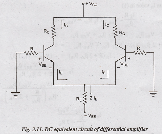
The
dc equivalent circuit can be obtained by setting the input voltages V1
and V2 of differential amplifier. The internal resistances are
denoted by R1 = R2 = R. The bases of both the transistors
are grounded through the resistors R and and their emitter are connected to
negative voltage -VEE
The
current through emitter resistor RE is equal to 2 IE
since their emitter currents are identical and both the transistors will
conduct simultaneously.
To
determine the operating point for the differential amplifier, we have to find
the values for IC and VCEQ
Apply
KVL to the base emitter loop of Q1 transistor from Fig. 3.11.

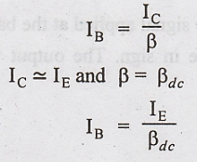
Substitute
IB value in (1)
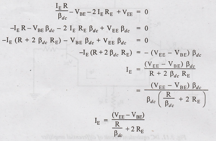
Generally 
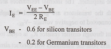
Under
dc conditions, the collector current is approximately equal to the emitter current.
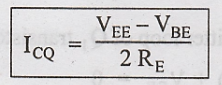
For
a given value of VEE, the emitter current IE and ICQ
is determined by the emitter resistance RE. The emitter current is
independent of the collector resistance RC. Then we have to find the
expression for VCEQ transistor Q1.
Assumption
The
voltage drop across the resistance R is negligibly small.
The
emitter voltage of Q1 is approximately equal to -VBE
Then


AC Analysis
The
ac analysis of the differential amplifier can be obtained using h-parameter
model. The ac analysis is done for only one transistor using h-parameters. We
are going to find
i. Differential gain, Ad
ii.
Common mode gain, Ac
iii.
Input impedance, Ri
iv.
Output impedance, RO
Fig.
3.12 shows the ac equivalent circuit for the differential amplifier, for ac
analysis, the two input signals are equal in magnitude and 180° out of phase
with respect to each other.
Assumption
i.
The input signals appearing across the terminals should be equal and 180° out
of phase.
ii.
V1 = V2 = Vin/2
iii.
The output signal at the emitter resistor RE is zero and hence it is
short circuited.
iv.
The emitter terminals connected to the ground.
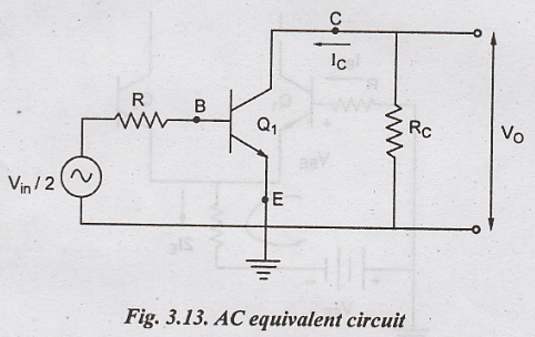
The
approximate h-parameter model for the ac equivalent circuit can be obtained as
shown in Fig.3.13.
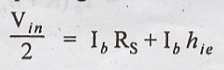
Applying
KVL to the input loop L1 of Fig. 3.14,
We
get,


Applying
KVL to the output loop L2


Substitute
Ib value in (1) in above equation

The
negative sign indicates that the input and output voltages are out of phase
with respect to each other.
i. Differential Gain
Ad
The
two input signals are equal in magnitude and opposite in phase. The differential
voltage is given by

The
differential gain, 
substitute
equation (2) in (3)

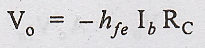
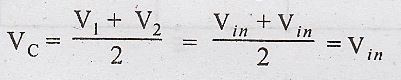
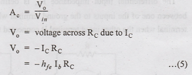
ii. Common Mode Gain
Ac
Let
the input to both the transistors are of the same magnitude and phase.
V1
= V2 = Vin
The
common mode input signal is the average of the two input signals.
The
output voltage is given as

The
emitter current will flow through the emitter resistance RE in both
the transistors. Thus, the ac current flowing through RE is equal to
2 IE.

Since
we are using the matched transistors, only one transistor is used for analysis.
The ac equivalent circuit for the common mode operation is shown in Fig. 3.15.
The
h-parameter equivalent circuit can be obtained as shown in Fig.3.16. The emitter
resistance is 2 RE due to the symmetry of the differential amplifier
circuit.

The
common mode gain Ac is defined as
Applying
KVL to the input circuit
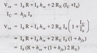
Substitute
(6) in (5)

iii. Common Mode
Rejection Ratio (CMRR)
CMRR
is defined as the ratio of differential gain to common mode gain.
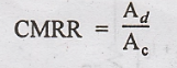
CMRR
of a differential amplifier should be as high as possible. To improve CMRR,
common mode gain Ac should be reduced. This can be achieved by increasing
the emitter resistance RE.
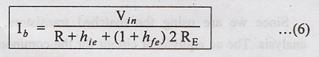
iv. Differential
Input Impedance (Rin)
The
differential input impedance Rin is defined as the equivalent
resistance between one of the inputs to the ground terminal when the other
input to the ground terminal when the other input terminal is connected to
ground.
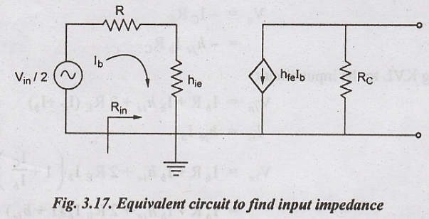
Applying
KVL to the input loop of Fig.3.17.

v. Output Impedance
(RO)
From
Fig.3.18, the expression for RO can be obtained as follows

The
input signal Vin is reduced to zero. This makes the base current Ib
to be zero. Therefore, hfe Ib = 0. Thus the current
source is equivalent to an open circuit.
The
output impedance is defined as the resistance measured between output terminals
to ground. In the circuit shown in Fig. 3.18, RO = RC.
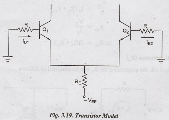
Input Bias Current
Assume
that both the inputs are connected to ground. Due to the emitter voltage - VEE,
both the transistors are forward biased and conduct simultaneously Q1
and Q2 are assumed to be as matched transistors. In practice, the
matching will not be perfect. So, the base currents IB1 and IB2
are not equal.
The
input bias current IB is defined as the average of the base currents
IB1 and IB2 flowing into the two transistors of the
differential amplifier.
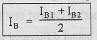
For
an ideal differential amplifier, the input bias current should be zero. But
practically it should be as small as possible.
Input Offset Current (Iios)
It
is defined as the algebraic difference between the base currents IB1
and IB2.

Iios
should be practically as small as possible.
Summary
1.
Differential voltage gain 
2.
Common mode voltage gain 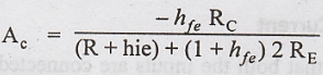
3.
Input Impedance 
4.
Output Impedance 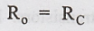
5.
Input bias current 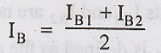

Electronic Devices and Circuits: Unit III: Multistage Amplifiers and Differential Amplifier : Tag: : Operation, Analysis, Summary - Basic Differential Amplifier
Related Topics
Related Subjects

Electronic Devices and Circuits
EC3353 - EDC - 3rd Semester - ECE Dept - 2021 Regulation | 3rd Semester ECE Dept 2021 Regulation